


 The Marketing Minute: Cracking the Code of Technical Marketing
 Trouble in Your Tank: Implementing Direct Metallization in Advanced Substrate Packaging


Filming Light and Electrons Coupled Together as They Travel Under Cover
October 13, 2016 | Ecole Polytechnique Fédérale de LausanneEstimated reading time: 2 minutes
In a breakthrough for future optical-electronic hybrid computers, scientists at EPFL have developed an ultrafast technique that can track light and electrons as they travel through a nanostructured surface.
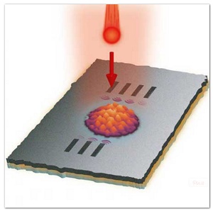
An illustration of the experimental set-up described in this study. (Image: F. Carbone/EPFL)
When light couples to electrons on a surface, their concerted motion can travel as a wave guided by the surface geometry itself. These waves are known as "surface plasmons" and might be useful in telecommunications and future computing, where data will be shuttled across processors using light instead of electricity. Aside from being more energy-efficient, these processors could be miniaturized down to the nanoscale to build high-resolution sensors and nanosized signal processing systems. But these processors would be built from stacking different layers of advanced materials and, so far, we don't have a reliable way of tracking the guided light as it moves across their interfaces.
EPFL scientists have now done exactly that using a new, ultrafast method. The breakthrough is published today in Nature Communications ("Imaging and controlling plasmonic interference fields at buried interfaces").
The lab of Fabrizio Carbone at EPFL led the project to create a tiny antenna array that would allow plasmons to travel across an interface. The array consisted of an extremely thin membrane of silicon nitride (50 nm thick) covered with an even thinner film of silver (30 nm thick). The scientists then "punched" a series of nano-holes through the surface that would act as the antennas -- the plasmon "hotspots".
The researchers then fired ultrafast laser pulses (light) onto the array to light up the antennas. With a controlled temporal delay, ultrashort electron pulses were then fired across the multilayer stack, to map the plasmons radiated by the antennas at the interface between the silver film and the silicon nitride membrane. Using an ultrafast technique called PINEM, which can "see" surface plasmons, even when they are bound to a buried interface, the scientists were able to actually film the propagation of the guided light and read its spatial profile across the film.
"Trying to see plasmons in these interfaces between layers is a bit like trying to film people in a house from the outside," explains Fabrizio Carbone. "A regular camera won't show you anything; but if you use microwave or a similar energy-tracking imaging, you can see right through the walls."
The current paper paves the way for designing and controlling confined plasmonic fields in multilayered structures, which is key for future optoelectronic devices.
Share on:


Testimonial
"We’re proud to call I-Connect007 a trusted partner. Their innovative approach and industry insight made our podcast collaboration a success by connecting us with the right audience and delivering real results."
Julia McCaffrey - NCAB GroupSuggested Items
Driving Innovation: Depth Routing Processes—Achieving Unparalleled Precision in Complex PCBs
09/08/2025 | Kurt Palmer -- Column: Driving InnovationIn PCB manufacturing, the demand for increasingly complex and miniaturized designs continually pushes the boundaries of traditional fabrication methods, including depth routing. Success in these applications demands not only on robust machinery but also sophisticated control functions. PCB manufacturers rely on advanced machine features and process methodologies to meet their precise depth routing goals. Here, I’ll explore some crucial functions that empower manufacturers to master complex depth routing challenges.
Polar Instruments Announces Additive Transmission Line Support for Si9000e
08/20/2025 | Polar InstrumentsTransmission lines embedded into the PCB surface are a feature of UHDI constructions. The 2025 fall release of Polar's Si9000e PCB impedance & insertion loss transmission line field solver incorporates eight new single ended, differential and coplanar transmission line structures.
Henniker Plasma Launches Stratus Turnkey Plasma Manufacturing Cell
08/13/2025 | Henniker PlasmaHenniker Plasma, a leading manufacturer of plasma treatment systems, proudly announces the launch of its Stratus Plasma Manufacturing Cell range — a fully integrated, turnkey solution that combines advanced atmospheric plasma surface treatment with robotic automation.
Trouble in Your Tank: Metallizing Flexible Circuit Materials—Mitigating Deposit Stress
08/04/2025 | Michael Carano -- Column: Trouble in Your TankMetallizing materials, such as polyimide used for flexible circuitry and high-reliability multilayer printed wiring boards, provide a significant challenge for process engineers. Conventional electroless copper systems often require pre-treatments with hazardous chemicals or have a small process window to achieve uniform coverage without blistering. It all boils down to enhancing the adhesion of the thin film of electroless copper to these smooth surfaces.
Designers Notebook: Basic PCB Planning Criteria—Establishing Design Constraints
07/22/2025 | Vern Solberg -- Column: Designer's NotebookPrinted circuit board development flows more smoothly when all critical issues are predefined and understood from the start. As a basic planning strategy, the designer must first consider the product performance criteria, then determine the specific industry standards or specifications that the product must meet. Planning also includes a review of all significant issues that may affect the product’s manufacture, performance, reliability, overall quality, and safety.