


 The Marketing Minute: Cracking the Code of Technical Marketing
 Trouble in Your Tank: Implementing Direct Metallization in Advanced Substrate Packaging


iPhone 7: Apple Underwent Strategic Change by Selecting TSMC’s inFO Platform
October 21, 2016 | Yole DéveloppementEstimated reading time: 2 minutes
Each year, Apple integrates more and more innovative technologies in its iPhone products. This year, with the new iPhone 7 and its A10 processor, the leading company is the first organization to bring out PoP WLP at the consumer scale. Apple underwent a strategic change by selecting TSMC’s new inFO-PoP packaging technology for its new A10 processor. Without doubt, this technical choice had a strong impact on the advanced packaging industry: according to Yole Développement (Yole), fan-out activity revenues forecast should reach about US$ 2.5 billion in 2021, with 80% growth between 2015 and 2017.
System Plus Consulting, proposes today a detailed technology analysis of Apple’s A10 processor, named TSMC Integrated Fan-Out (inFO) Package in Apple’s A10 Application Processor. Under this report, the reverse engineering and costing company provides a comprehensive understanding of the A10 manufacturing processes as well as accurate estimations of manufacturing costs and selling prices. With more than 100 relevant technical and strategic analyses per year, System Plus Consulting analysts combine their technical, marketing, reverse engineering and costing know-how in the “More than Moore” semiconductor industry, to be at the cutting edge of innovation and the most recent technologies and provide deep added-value analysis.
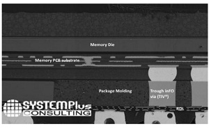
IPhone 7 & A10 application processor: what’s inside?
Located on the main board, A10 application processor (bottom package) and the DRAM Chip (top package) have been developed in a PoP configuration. Depending on the version, iPhone 7 or iPhone 7 Plus, the DRAM memory has different space management. Apple’s A10 is a wafer-level package using TSMC’s packaging technology with copper pillar Through inFO Vias. This technology is replacing the well-known Through Molded Via approach. “With this new technology, Apple has made a huge break from traditional PoP packaging found in previous AP generations”, asserts Stéphane Elisabeth, RF and Advanced Packaging Cost Engineer at System Plus Consulting.
In this report, System Plus Consulting highlights Apple’s latest innovations at the packaging level. Indeed the company is offering an in-depth analysis of the package process including copper pillars, redistribution layer, and silicon high density capacitor integration. The deep trench capacitor is the first integrated component developed by TSMC for high-volume consumer applications. System Plus Consulting had also available a detail report on this capacitor.
A detailed comparison has been performed by System Plus Consulting’s experts and especially the pros and cons of inFO technology compared to PoP packaging selected by Samsung for its Exynos 8 processor and by Qualcomm for the development of its Snapdragon 820 processor (for Samsung as well).
Thanks to the inFO process, Apple is able today to offer a very thin package on package, with a high number of I/O pads and better thermal management. According to System Plus Consulting’s report, the A10 processor is showing an impressive thickness reduction of 30% compared to traditional PoP-based systems. In addition, TSMC removed a lot of expensive manufacturing steps. “The result is a very cost-effective component that can compete with any well-known PoP” comments Stéphane Elisabeth from System Plus Consulting.
The new reverse engineering and costing report from System Plus Consulting compares costs with other chips and includes a technical comparison with the previous Apple AP, the A9.
Share on:


Testimonial
"The I-Connect007 team is outstanding—kind, responsive, and a true marketing partner. Their design team created fresh, eye-catching ads, and their editorial support polished our content to let our brand shine. Thank you all! "
Sweeney Ng - CEE PCBSuggested Items
Trouble in Your Tank: Implementing Direct Metallization in Advanced Substrate Packaging
09/15/2025 | Michael Carano -- Column: Trouble in Your TankDirect metallization systems based on conductive graphite are gaining popularity throughout the world. The environmental and productivity gains achievable with this process are outstanding. Direct metallization reduces the costs of compliance, waste treatment, and legal issues related to chemical exposure. A graphite-based direct plate system has been devised to address these needs.
Closing the Loop on PCB Etching Waste
09/09/2025 | Shawn Stone, IECAs the PCB industry continues its push toward greener, more cost-efficient operations, Sigma Engineering’s Mecer System offers a comprehensive solution to two of the industry’s most persistent pain points: etchant consumption and rinse water waste. Designed as a modular, fully automated platform, the Mecer System regenerates spent copper etchants—both alkaline and acidic—and simultaneously recycles rinse water, transforming a traditionally linear chemical process into a closed-loop system.
Driving Innovation: Depth Routing Processes—Achieving Unparalleled Precision in Complex PCBs
09/08/2025 | Kurt Palmer -- Column: Driving InnovationIn PCB manufacturing, the demand for increasingly complex and miniaturized designs continually pushes the boundaries of traditional fabrication methods, including depth routing. Success in these applications demands not only on robust machinery but also sophisticated control functions. PCB manufacturers rely on advanced machine features and process methodologies to meet their precise depth routing goals. Here, I’ll explore some crucial functions that empower manufacturers to master complex depth routing challenges.
Trouble in Your Tank: Minimizing Small-via Defects for High-reliability PCBs
08/27/2025 | Michael Carano -- Column: Trouble in Your TankTo quote the comedian Stephen Wright, “If at first you don’t succeed, then skydiving is not for you.” That can be the battle cry when you find that only small-diameter vias are exhibiting voids. Why are small holes more prone to voids than larger vias when processed through electroless copper? There are several reasons.
The Government Circuit: Navigating New Trade Headwinds and New Partnerships
08/25/2025 | Chris Mitchell -- Column: The Government CircuitAs global trade winds continue to howl, the electronics manufacturing industry finds itself at a critical juncture. After months of warnings, the U.S. Government has implemented a broad array of tariff increases, with fresh duties hitting copper-based products, semiconductors, and imports from many nations. On the positive side, tentative trade agreements with Europe, China, Japan, and other nations are providing at least some clarity and counterbalance.