


 Flexible Thinking: Designing Flex Circuits for Dynamic Reliability
 Global PCB Connections: Rigid-flex and Flexible PCBs—The Backbone of Modern Electronics
 Happy’s Tech Talk #29: Bend-to-Install Semi-flex FR-4


Ventec Celebrates a Decade of Innovation, Excellence and Business Growth at electronica
October 24, 2016 | Ventec International GroupEstimated reading time: 2 minutes
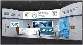
Ventec International Group is excited to have reached its 10-year European anniversary as a world leader in the production of polyimide & high reliability epoxy laminates and prepregs. Ventec will be celebrating this important milestone at electronica, November 8-11 in Munich, Germany on Booth B4/118.
Incorporated in November 2006 as a joint venture known as Global Ventec Laminates, Ventec Europe imported its first container-full of material in May 2007 and later that year began cutting, packaging and shipping material from its original location in Leamington Spa, England. The company has expanded considerably over the past decade and today is operating two fully equipped service & warehousing centres in the UK and Germany and further sales and service offices in France, Italy and Holland. The UK facility operates two state-of-the-art Yow Shi diamond blade saws with full extraction and three state-of-the-art Pasquato slitters, one dedicated to polyimide. All the machines are equipped with certified Class 1000 laminar flow canopies, and the company maintains a strict clean-room cutting environment. The German facility, which opened in 2010, operates a large-format Holzma panel saw for volume production and a similar Pasquato machine as in the UK. Ventec’s UK centre is certified to AS9100 Rev C, and all facilities operate to ISO 9001:2015 standards.
Crucially, Ventec’s success in Europe sparked the company's global expansion through further facilities in the East and West Coast and Mid-West of America as well as penetration into well-established high-reliability markets like Israel, and into the OEM market with its IMS business. Today, Ventec has built a reputation as an industry leader with an overseas business approaching 50 million dollars.
At electronica 2016, Ventec's expert team will be on hand on Booth B4/118 throughout the show. Show-highlights include:
- Latest advances in high performance IMS materials that deliver an exceptional thermal performance, reliability and quality, particularly demanded by automotive and other LED lighting and DC power conversion applications;
- Latest developments in polyimide technology;
- Ventec's advanced high speed/low loss product line 'tec-speed';
- Newest ranges of PCB base-materials including complementary products such as flex- & rigid-flex circuit board materials, back-up, entry & routing materials, foils and coatings;
- Ventec 10th Anniversary Booth Party – a relaxed and informal celebration with the Ventec Team on Wednesday, 9th November from 6pm on Booth B4/118.
"Ventec is proud of its ten-year track record of successful growth and sustained profitability" said Mark Goodwin, COO USA & Europe. "At the same time, we are forward-focused on the next decade and have significant strategic plans to continue to deliver future proof materials and services as we see an increase in demand for Ventec solutions."
For more information about Ventec's solutions and the company’s wide variety of products, please visit www.venteclaminates.com.
For more information on the company's vision for the future, and to meet Ventec Europe co-founder Mark Goodwin (COO, Europe & USA), Thomas Michels (Managing Director, Europe) or other members of the Ventec team, please contact Kim Sauer (kim@wearescoop.com) to arrange an appointment at electronica.
About Ventec International Group
With volume manufacturing facilities and HQ in Suzhou China, Ventec International specializes in advanced copper clad glass reinforced and metal backed substrates for the PCB industry. With distribution locations and quick-turn CCL manufacturing sites in both the US and Europe, Ventec International is a premier supplier to the Global PCB industry. For more information, click here.
Share on:


Testimonial
"We’re proud to call I-Connect007 a trusted partner. Their innovative approach and industry insight made our podcast collaboration a success by connecting us with the right audience and delivering real results."
Julia McCaffrey - NCAB GroupSuggested Items
Driving Innovation: Selecting the Right Laser Source
04/28/2026 | Simon Khesin -- Column: Driving InnovationWhen I first joined Schmoll Maschinen, I brought experience from almost every PCB process, except for laser. As I immersed myself in laser processing, I realized why it can seem so daunting to a newcomer. The complexity arises from three intersecting factors: A vast variety of laser sources: CO2, UV-nano, green-pico, UV-pico, IR-pico, and others; a diverse range of applications: Drilling, cutting, ablation, and more; and an extensive list of materials: These have vastly different absorption rates. Choosing the right machine or laser source is rarely trivial. Even for experienced engineers, answering "Which source is best?" requires examining the business's specific goals.
Institute of Circuit Technology Spring Seminar 2026: A Bright Future in Europe
04/23/2026 | Pete Starkey, I-Connect007Through the leafy lanes and spring flowers of Warwickshire and back to Meridan, the traditional centre of England, and now officially part of the Metropolitan Borough of Solihull in the county of the West Midlands, I attended the Annual General Meeting and Spring Seminar of the Institute of Circuit Technology (ICT) on April 14. Out of the AGM came notable changes in leadership at the top of the Institute: the retirement of Mat Beadel as chair and Emma Hudson as technical director. Effective May 1, Steve Driver is the new chair, and Alun Morgan is the new technical director.
ACCM Unveils Negative and Near-zero CTE Materials for Large-Format AI Chips
04/21/2026 | Advanced Chip and Circuit MaterialsAdvanced Chip and Circuit Materials, Inc. (ACCM) has launched two new materials: Celeritas HM50, with a negative coefficient of thermal expansion (CTE) of -8 ppm/°C to offset the positive CTE and expansion of copper with temperature on circuit boards, and Celeritas HM001, with near-zero CTE and the low-loss performance needed for high-speed signal layers to 224 Gb/s and faster in artificial intelligence (AI) circuits.
Fresh PCB Concepts: Designing PCBs for Harsh Environments—Reliability Is Engineered Upstream
04/23/2026 | Team NCAB -- Column: Fresh PCB ConceptsWhen engineers hear the phrase “harsh environment,” they usually think of the extreme temperature swings, vibration and shock, pressure changes, or radiation in aerospace. However, aerospace is not the only harsh environment where electronic assemblies must survive. Automotive power electronics, downhole oil and gas tools, marine controls, rail systems, defense platforms, and industrial automation equipment all expose PCBs to environments that are equally unforgiving. The stress mechanisms may differ, but the physics does not.
Advanced Packaging for AI: Reliability Starts at the Cu/Cu/Cu Microvia Junction
04/20/2026 | Kuldip Johal, MKS' AtotechThe rapid growth of AI computing, from training clusters to inference at scale, is reshaping demand across the entire electronics supply chain. Advances in technology requirements, such as higher bandwidth, lower latency, and greater compute density, are driving the development of advanced packaging technologies and transforming the PCB industry across design, manufacturing, testing, and even architecture.