


 The Marketing Minute: Cracking the Code of Technical Marketing
 Trouble in Your Tank: Implementing Direct Metallization in Advanced Substrate Packaging


Controlling the Properties of Matter in Two-Dimensional Crystals
October 27, 2016 | Penn State Materials Research InstituteEstimated reading time: 3 minutes
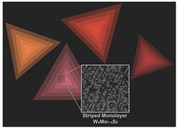
By creating atomic chains in a two-dimensional crystal, researchers at Penn State believe they have found a way to control the direction of materials properties in two and three dimensional crystals with implications in sensing, optoelectronics and next-generation electronics applications ("Spontaneous formation of atomically thin stripes in transition metal dichalcogenide monolayers").
Whether an alloy has a random arrangement of atoms or one that is ordered can have large effects on a material’s properties. In a new paper published online in the journal Nano Letters, Nasim Alem, assistant professor of materials science and engineering, and colleagues at Penn State used a combination of simulations and scanning transmission electron microscopy imaging to determine the atomic structure of an ordered alloy of molybdenum, tungsten and sulfur. They determined that fluctuations in the amount of available sulfur were responsible for the creation of atomic chains of either molybdenum or tungsten.
An electron microscopy image of ordered atoms of tungsten (W) and molybdenum (Mo) against artistic representations of triangular single layer flakes of WxMo1–xS2 on a substrate
An electron microscopy image of ordered atoms of tungsten (W) and molybdenum (Mo) against artistic representations of triangular single layer flakes of WxMo1–xS2 on a substrate. (Amin Azizi and Andrea Kohler/Penn State)
“We discovered how chains form in a two-dimensional alloy as a result of fluctuations in the amount of a particular precursor, in this case sulfur,” Alem said. “Normally, when we combine atoms of different elements, we don’t know how to control where the atoms will go. But we have found a mechanism to give order to the atoms, which in turn introduces control of the properties, not only heat transport, as is the case in this work, but also electronic, chemical or magnetic properties in other alloy cases. If you know the mechanism, you can apply it to arrange the atoms in a wide range of alloys in 2D crystals across the Periodic Table.”
In the case of the molybdenum, tungsten and sulfur alloy, they showed that the electronic properties were the same in every direction, but using simulations they predict that the thermal transport properties are smaller perpendicular to the chains or stripes.
“We didn’t know why this crystal forms an ordered structure, so we worked with my colleague Dr. Vin Crespi to understand the underlying physics that causes order in this crystal. Our calculations show it was the fluctuations in the third element, sulfur, that was determining how the chains formed,” Alem said.
Vincent H. Crespi, Distinguished Professor of Physics, and professor of chemistry and materials science and engineering who developed the theoretical understanding of the phenomenon, said, "Although the interior of the flake is indifferent to whether molybdenum or tungsten occupies any site in the crystal lattice, the edge of the growing crystal does care: Depending on how much sulfur is available at a given location, the edge will prefer to be either 100% molybdenum or 100% tungsten. So as the availability of sulfur randomly varies during growth, the system alternately lays down rows of molybdenum or tungsten. We think this may be a general mechanism to create stripe-like structures in 2D materials."
Amin Aziz, who is a Ph.D. candidate in Alem’s group and lead author on the Nano Letters paper, produced the STEM imaging and spectroscopy that showed the fine atomic structure of the alloy samples and their electronic properties.
“When we are able to directly image constitutive atoms of a substance, see how they interact with each other at the atomic level and try to understand the origins of such behaviors, we could potentially create new materials with unusual properties that have never existed,” said Azizi.
A team led by Mauricio Terrones, professor of physics, produced samples of this ordered alloy by vaporizing powders of all three elements, called precursors, under high heat.
Share on:


Testimonial
"The I-Connect007 team is outstanding—kind, responsive, and a true marketing partner. Their design team created fresh, eye-catching ads, and their editorial support polished our content to let our brand shine. Thank you all! "
Sweeney Ng - CEE PCBSuggested Items
Curing and Verification in PCB Shadow Areas
09/17/2025 | Doug Katze, DymaxDesign engineers know a simple truth that often complicates electronics manufacturing: Light doesn’t go around corners. In densely populated PCBs, adhesives and coatings often fail to fully cure in shadowed regions created by tall ICs, connectors, relays, and tight housings.
Marcy’s Musings: Advancing the Advanced Materials Discussion
09/17/2025 | Marcy LaRont -- Column: Marcy's MusingsAs the industry’s most trusted global source of original content about the electronics supply chain, we continually ask you about your concerns, what you care about, and what you most want to learn about. Your responses are insightful and valuable. Thank you for caring enough to provide useful feedback and engage in dialogue.
September 2025 PCB007 Magazine: The Future of Advanced Materials
09/16/2025 | I-Connect007 Editorial TeamMoore’s Law is no more, and the advanced material solutions being developed to grapple with this reality are surprising, stunning, and perhaps a bit daunting. Buckle up for a dive into advanced materials and a glimpse into the next chapters of electronics manufacturing.
I-Connect007 Launches Advanced Electronics Packaging Digest
09/15/2025 | I-Connect007I-Connect007 is pleased to announce the launch of Advanced Electronics Packaging Digest (AEPD), a new monthly digital newsletter dedicated to one of the most critical and rapidly evolving areas of electronics manufacturing: advanced packaging at the interconnect level.
Panasonic Industry will Double the Production Capacity of MEGTRON Multi-layer Circuit Board Materials Over the Next Five Years
09/15/2025 | Panasonic Industry Co., Ltd.Panasonic Industry Co., Ltd., a Panasonic Group company, announced plans for a major expansion of its global production capacity for MEGTRON multi-layer circuit board materials today. The company plans to double its production over the next five years to meet growing demand in the AI server and ICT infrastructure markets.