


 The Marketing Minute: Cracking the Code of Technical Marketing
 Trouble in Your Tank: Implementing Direct Metallization in Advanced Substrate Packaging


A Tiny Machine
October 31, 2016 | UC Santa BarbaraEstimated reading time: 3 minutes
In 1959 renowned physicist Richard Feynman, in his talk “Plenty of Room at the Bottom,” spoke of a future in which tiny machines could perform huge feats. Like many forward-looking concepts, his molecule and atom-sized world remained for years in the realm of science fiction.
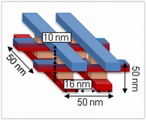
A figure depicting the structure of stacked memristors with dimensions that could satisfy the Feynman Grand Challenge
And then, scientists and other creative thinkers began to realize Feynman’s nanotechnological visions.
In the spirit of Feynman’s insight, and in response to the challenges he issued as a way to inspire scientific and engineering creativity, electrical and computer engineers at UC Santa Barbara have developed a design for a functional nanoscale computing device. The concept involves a dense, three-dimensional circuit operating on an unconventional type of logic that could, theoretically, be packed into a block no bigger than 50 nanometers on any side.
“Novel computing paradigms are needed to keep up with the demand for faster, smaller and more energy-efficient devices,” said Gina Adam, postdoctoral researcher at UCSB’s Department of Computer Science and lead author of the paper “Optimized stateful material implication logic for three dimensional data manipulation,” published in the journal Nano Research. “In a regular computer, data processing and memory storage are separated, which slows down computation. Processing data directly inside a three-dimensional memory structure would allow more data to be stored and processed much faster.”
While efforts to shrink computing devices have been ongoing for decades — in fact, Feynman’s challenges as he presented them in his 1959 talk have been met — scientists and engineers continue to carve out room at the bottom for even more advanced nanotechnology. A nanoscale 8-bit adder operating in 50-by-50-by-50 nanometer dimension, put forth as part of the current Feynman Grand Prize challenge by the Foresight Institute, has not yet been achieved. However, the continuing development and fabrication of progressively smaller components is bringing this virus-sized computing device closer to reality, said Dmitri Strukov, a UCSB professor of computer science.
“Our contribution is that we improved the specific features of that logic and designed it so it could be built in three dimensions,” he said.
Key to this development is the use of a logic system called material implication logic combined with memristors — circuit elements whose resistance depends on the most recent charges and the directions of those currents that have flowed through them. Unlike the conventional computing logic and circuitry found in our present computers and other devices, in this form of computing, logic operation and information storage happen simultaneously and locally. This greatly reduces the need for components and space typically used to perform logic operations and to move data back and forth between operation and memory storage. The result of the computation is immediately stored in a memory element, which prevents data loss in the event of power outages — a critical function in autonomous systems such as robotics.
In addition, the researchers reconfigured the traditionally two-dimensional architecture of the memristor into a three-dimensional block, which could then be stacked and packed into the space required to meet the Feynman Grand Prize Challenge.
“Previous groups show that individual blocks can be scaled to very small dimensions, let’s say 10-by-10 nanometers,” said Strukov, who worked at technology company Hewlett-Packard’s labs when they ramped up development of memristors and material implication logic. By applying those results to his group’s developments, he said, the challenge could easily be met.
The tiny memristors are being heavily researched in academia and in industry for their promising uses in memory storage and neuromorphic computing. While implementations of material implication logic are rather exotic and not yet mainstream, uses for it could pop up any time, particularly in energy scarce systems such as robotics and medical implants.
“Since this technology is still new, more research is needed to increase its reliability and lifetime and to demonstrate large scale three-dimensional circuits tightly packed in tens or hundreds of layers,” Adam said.
Share on:


Testimonial
"Our marketing partnership with I-Connect007 is already delivering. Just a day after our press release went live, we received a direct inquiry about our updated products!"
Rachael Temple - AlltematedSuggested Items
Soaring Inference AI Demand Triggers Severe Nearline HDD Shortages; QLC SSD Shipments Poised for Breakout in 2026
09/16/2025 | TrendForceTrendForce’s latest investigations reveal that the massive data volumes generated by AI are straining the global infrastructure of data center storage.
Advanced Packaging-to-Board-Level Integration: Needs and Challenges
09/15/2025 | Devan Iyer and Matt Kelly, Global Electronics AssociationHPC data center markets now demand components with the highest processing and communication rates (low latencies and high bandwidth, often both simultaneously) and highest capacities with extreme requirements for advanced packaging solutions at both the component level and system level. Insatiable demands have been projected for heterogeneous compute, memory, storage, and data communications. Interconnect has become one of the most important pillars of compute for these systems.
Procense Raises $1.5M in Seed Funding to Accelerate AI-Powered Manufacturing
09/11/2025 | BUSINESS WIREProcense, a San Francisco-based industrial automation startup developing cutting-edge AI and remote sensing technologies for process manufacturers has raised $1.5 million in a seed funding round led by Kevin Mahaffey, Business Insider’s #1 seed investor of 2025 and HighSage Ventures, a Boston-based family office that primarily invests in public and private companies in the global software, internet, consumer, and financial technology sectors.
Zuken Announces E3.series 2026 Release for Accelerated Electrical Design and Enhanced Engineering Productivity
09/10/2025 | ZukenZuken reveals details of the upcoming 2026 release of E3.series, which will introduce powerful new features aimed at streamlining electrical and fluid design, enhancing multi-disciplinary collaboration, and boosting engineering productivity.
AI Infrastructure Boosts Global Semiconductor Revenue Growth to 17.6% in 2025
09/09/2025 | IDCAccording to the Worldwide Semiconduct o r Technology and Supply Chain Intelligence service from International Data Corporation (IDC), worldwide semiconductor revenue is expected to reach $800 billion in 2025, growing 17.6% year-over-year from $680 billion in 2024. This follows a strong rebound in 2024, when revenue grew by 22.4% year-over-year.