


 The Marketing Minute: Cracking the Code of Technical Marketing
 Trouble in Your Tank: Implementing Direct Metallization in Advanced Substrate Packaging
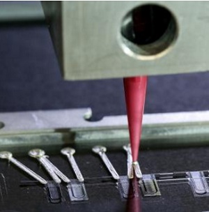


3D-printed Heart-on-a-chip with Integrated Sensors
November 1, 2016 | Harvard School of Engineering and Applied SciencesEstimated reading time: 3 minutes
Harvard University researchers have made the first entirely 3D-printed organ-on-a-chip with integrated sensing. Built by a fully automated, digital manufacturing procedure, the 3D-printed heart-on-a-chip can be quickly fabricated and customized, allowing researchers to easily collect reliable data for short-term and long-term studies.
This new approach to manufacturing may one day allow researchers to rapidly design organs-on-chips, also known as microphysiological systems, that match the properties of a specific disease or even an individual patient’s cells.
“This new programmable approach to building organs-on-chips not only allows us to easily change and customize the design of the system but also drastically simplifies data acquisition,” said Johan Ulrik Lind, first author of the paper and postdoctoral fellow at the Harvard John A. Paulson School of Engineering and Applied Sciences (SEAS). Lind is also a researcher at the Wyss Institute for Biologically Inspired Engineering at Harvard University.
“Our microfabrication approach opens new avenues for in vitro tissue engineering, toxicology and drug screening research,” said Kit Parker, Tarr Family Professor of Bioengineering and Applied Physics at SEAS, who coauthored the study. Parker is also a Core Faculty Member of the Wyss Institute.
Organs-on-chips mimic the structure and function of native tissue and have emerged as a promising alternative to traditional animal testing. Harvard researchers have developed microphysiological systems that mimic the microarchitecture and functions of lungs, hearts, tongues and intestines.
However, the fabrication and data collection process for organs-on-chips is expensive and laborious. Currently, these devices are built in clean rooms using a complex, multi-step lithographic process and collecting data requires microscopy or high-speed cameras.
“Our approach was to address these two challenges simultaneously via digital manufacturing,” said Travis Busbee, coauthor of the paper and graduate student in the Lewis Lab. “By developing new printable inks for multi-material 3D printing, we were able to automate the fabrication process while increasing the complexity of the devices.”
The researchers developed six different inks that integrated soft strain sensors within the micro-architecture of the tissue. In a single, continuous procedure, the team 3D printed those materials into a cardiac microphysiological device — a heart on a chip — with integrated sensors.
“We are pushing the boundaries of three-dimensional printing by developing and integrating multiple functional materials within printed devices,” said Jennifer Lewis, Hansjorg Wyss Professor of Biologically Inspired Engineering, and coauthor of the study. “This study is a powerful demonstration of how our platform can be used to create fully functional, instrumented chips for drug screening and disease modeling.”
Lewis is also a Core Faculty Member of the Wyss Institute.
The chip contains multiple wells, each with separate tissues and integrated sensors, allowing researchers to study many engineered cardiac tissues at once. To demonstrate the efficacy of the device, the team performed drug studies and longer-term studies of gradual changes in the contractile stress of engineered cardiac tissues, which can occur over the course of several weeks.
“Researchers are often left working in the dark when it comes to gradual changes that occur during cardiac tissue development and maturation because there has been a lack of easy, non-invasive ways to measure the tissue functional performance,” said Lind. “These integrated sensors allow researchers to continuously collect data while tissues mature and improve their contractility. Similarly, they will enable studies of gradual effects of chronic exposure to toxins.”
“Translating microphysiological devices into truly valuable platforms for studying human health and disease requires that we address both data acquisition and manufacturing of our devices,” said Parker. “This work offers new potential solutions to both of these central challenges.”
This work was supported by the National Science Foundation, the National Center for Advancing Translational Sciences of the National Institutes of Health, the US Army Research Laboratory and the US Army Research, and the Harvard University Materials Research Science and Engineering Center (MRSEC).
Share on:


Testimonial
"Advertising in PCB007 Magazine has been a great way to showcase our bare board testers to the right audience. The I-Connect007 team makes the process smooth and professional. We’re proud to be featured in such a trusted publication."
Klaus Koziol - atgSuggested Items
Soaring Inference AI Demand Triggers Severe Nearline HDD Shortages; QLC SSD Shipments Poised for Breakout in 2026
09/16/2025 | TrendForceTrendForce’s latest investigations reveal that the massive data volumes generated by AI are straining the global infrastructure of data center storage.
Advanced Packaging-to-Board-Level Integration: Needs and Challenges
09/15/2025 | Devan Iyer and Matt Kelly, Global Electronics AssociationHPC data center markets now demand components with the highest processing and communication rates (low latencies and high bandwidth, often both simultaneously) and highest capacities with extreme requirements for advanced packaging solutions at both the component level and system level. Insatiable demands have been projected for heterogeneous compute, memory, storage, and data communications. Interconnect has become one of the most important pillars of compute for these systems.
Procense Raises $1.5M in Seed Funding to Accelerate AI-Powered Manufacturing
09/11/2025 | BUSINESS WIREProcense, a San Francisco-based industrial automation startup developing cutting-edge AI and remote sensing technologies for process manufacturers has raised $1.5 million in a seed funding round led by Kevin Mahaffey, Business Insider’s #1 seed investor of 2025 and HighSage Ventures, a Boston-based family office that primarily invests in public and private companies in the global software, internet, consumer, and financial technology sectors.
Zuken Announces E3.series 2026 Release for Accelerated Electrical Design and Enhanced Engineering Productivity
09/10/2025 | ZukenZuken reveals details of the upcoming 2026 release of E3.series, which will introduce powerful new features aimed at streamlining electrical and fluid design, enhancing multi-disciplinary collaboration, and boosting engineering productivity.
AI Infrastructure Boosts Global Semiconductor Revenue Growth to 17.6% in 2025
09/09/2025 | IDCAccording to the Worldwide Semiconduct o r Technology and Supply Chain Intelligence service from International Data Corporation (IDC), worldwide semiconductor revenue is expected to reach $800 billion in 2025, growing 17.6% year-over-year from $680 billion in 2024. This follows a strong rebound in 2024, when revenue grew by 22.4% year-over-year.