


 The Marketing Minute: Cracking the Code of Technical Marketing
 Trouble in Your Tank: Implementing Direct Metallization in Advanced Substrate Packaging


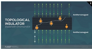
NIST Collaboration Heats Up Exotic Topological Insulators
November 2, 2016 | NISTEstimated reading time: 3 minutes
Fashion is changing in the avant-garde world of next-generation computer component materials. Traditional semiconductors like silicon are releasing their last new lines. Exotic materials called topological insulators (TIs) are on their way in. And when it comes to cool, nitrogen is the new helium.
This topological insulator, doped with chromium (Cr) atoms, conducts electricity on its surface and possesses desirable magnetic properties at a higher range of temperatures than before when sandwiched between magnetic materials known as ferromagnets.
This was clearly on display in a novel experiment (link is external) at the National Institute of Standards and Technology (NIST) that was performed by a multi-institutional collaboration including UCLA, NIST and the Beijing Institute of Technology in China.
Topological insulators are a new class of materials that were discovered less than a decade ago (link is external) after earlier theoretical work, recognized in the 2016 Nobel Prize in physics (link is external), predicted they could exist. The materials are electrical insulators on the inside and they conduct electricity on the outer surface. They are exciting to computer designers because electric current travels along them without shedding heat, meaning components made from them could reduce the high heat production that plagues modern computers. They also might be harnessed one day in quantum computers, which would exploit less familiar properties of electrons, such as their spin, to make calculations in entirely new ways. When TIs conduct electricity, all of the electrons flowing in one direction have the same spin, a useful property that quantum computer designers could harness.
The special properties that make TIs so exciting for technologists are usually observed only at very low temperature, typically requiring liquid helium to cool the materials. Not only does this demand for extreme cold make TIs unlikely to find use in electronics until this problem is overcome, but it also makes it difficult to study them in the first place.
Furthermore, making TIs magnetic is key to developing exciting new computing devices with them. But even getting them to the point where they can be magnetized is a laborious process. Two ways to do this have been to infuse, or “dope,” the TI with a small amount of magnetic metal and/or to stack thin layers of TI between alternating layers of a magnetic material known as a ferromagnet. However, increasing the doping to push the temperature higher disrupts the TI properties, while the alternate layers’ more powerful magnetism can overwhelm the TIs, making them hard to study.
To get around these problems, UCLA scientists tried a different substance for the alternating layers: an antiferromagnet. Unlike the permanent magnets on your fridge, whose atoms all have north poles that point in the same direction, the multilayered antiferromagnetic (AFM) materials had north poles pointing one way in one layer, and the opposite way in the next layer. Because these layers’ magnetism cancels each other out, the overall AFM doesn’t have net magnetism—but a single layer of its molecules does. It was the outermost layer of the AFM that the UCLA team hoped to exploit.
Fortunately, they found that the outermost layer’s influence magnetizes the TI, but without the overwhelming force that the previously used magnetic materials would bring. And they found that the new approach allowed the TIs to become magnetic and demonstrate all of the TI’s appealing hallmarks at temperatures far above 77 Kelvin—still too cold for use as consumer electronics components, but warm enough that scientists can use nitrogen to cool them instead.
“It makes them far easier to study,” said Alex Grutter of the NIST Center for Neutron Research, which partnered with the UCLA scientists to clarify the interactions between the overall material’s layers as well as its spin structure. “Not only can we explore TIs’ properties more easily, but we’re excited because to a physicist, finding one way to increase the operational temperature this dramatically suggests there might be other accessible ways to increase it again. Suddenly, room temperature TIs don’t look as far out of reach.”
Share on:


Testimonial
"In a year when every marketing dollar mattered, I chose to keep I-Connect007 in our 2025 plan. Their commitment to high-quality, insightful content aligns with Koh Young’s values and helps readers navigate a changing industry. "
Brent Fischthal - Koh YoungSuggested Items
Curing and Verification in PCB Shadow Areas
09/17/2025 | Doug Katze, DymaxDesign engineers know a simple truth that often complicates electronics manufacturing: Light doesn’t go around corners. In densely populated PCBs, adhesives and coatings often fail to fully cure in shadowed regions created by tall ICs, connectors, relays, and tight housings.
Marcy’s Musings: Advancing the Advanced Materials Discussion
09/17/2025 | Marcy LaRont -- Column: Marcy's MusingsAs the industry’s most trusted global source of original content about the electronics supply chain, we continually ask you about your concerns, what you care about, and what you most want to learn about. Your responses are insightful and valuable. Thank you for caring enough to provide useful feedback and engage in dialogue.
September 2025 PCB007 Magazine: The Future of Advanced Materials
09/16/2025 | I-Connect007 Editorial TeamMoore’s Law is no more, and the advanced material solutions being developed to grapple with this reality are surprising, stunning, and perhaps a bit daunting. Buckle up for a dive into advanced materials and a glimpse into the next chapters of electronics manufacturing.
I-Connect007 Launches Advanced Electronics Packaging Digest
09/15/2025 | I-Connect007I-Connect007 is pleased to announce the launch of Advanced Electronics Packaging Digest (AEPD), a new monthly digital newsletter dedicated to one of the most critical and rapidly evolving areas of electronics manufacturing: advanced packaging at the interconnect level.
Panasonic Industry will Double the Production Capacity of MEGTRON Multi-layer Circuit Board Materials Over the Next Five Years
09/15/2025 | Panasonic Industry Co., Ltd.Panasonic Industry Co., Ltd., a Panasonic Group company, announced plans for a major expansion of its global production capacity for MEGTRON multi-layer circuit board materials today. The company plans to double its production over the next five years to meet growing demand in the AI server and ICT infrastructure markets.