


 The Marketing Minute: Cracking the Code of Technical Marketing
 Trouble in Your Tank: Implementing Direct Metallization in Advanced Substrate Packaging


Prototype Device for Measuring Graphene-Based Electromagnetic Radiation Created
November 3, 2016 | Lomonosov Moscow State UniversityEstimated reading time: 1 minute
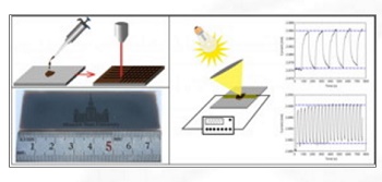
Bolometer is a device for measuring electromagnetic radiation energy flow based on measurement of variations of physical parameters of thermosensitive element as a result of heating by absorption of radiation energy.
"We studied thermal and optical properties of the carbon structures derived from the reduced graphene oxide in a wide range of wavelengths from visible to infrared. In addition to the optical and thermal properties of the carbon structures, we have demonstrated the bolometer prototype that operates at room temperature without additional cooling", says Stanislav Evlashin, the first author of the article, the researcher of the Skobeltsyn Institute of Nuclear Physics Lomonosov Moscow State University (SINP MSU), PhD in Physico-Mathematical Sciences.
Synthesis and investigations of the new materials for bolometric sensors have a great scientific and practical importance. Such materials should possess a high effective absorption over a wide spectral range, high stable thermoresistive effect (change in electrical conductance with temperature), and, of course, they must be cheap to manufacture.
To create bolometer prototype the water solution of graphene oxide was used, which was obtained by the standard method of graphite oxidation, which is known and widely used. The resulting suspension of graphene oxide was deposited on the substrate for subsequent laser microstructuring. Laser treatment causes partial reduction of graphene oxide film and changes morphology, consequently, it changes optical and thermal properties of graphene oxide.
The material synthesis and development of the bolometer prototype was held at SINP MSU. Studies on the optical properties were carried out at Physics Department of Moscow State University. Research on the thermal properties were carried out at LPI RAS.
"Laser microstructuring of graphene oxide opens up the possibility of selective creation of antireflective, thermally-conductive and electrically-conductive coatings. Developed method is quite cheap, compatible with conventional semiconductor technology and allows you to create antiabsorbing coatings that would cover large areas on almost any surface. The observed properties of reduced graphene oxide partially show the prospects of it's use in bolometric matrices and other IR devices," - says Stanislav Evlashin.
Share on:


Testimonial
"Advertising in PCB007 Magazine has been a great way to showcase our bare board testers to the right audience. The I-Connect007 team makes the process smooth and professional. We’re proud to be featured in such a trusted publication."
Klaus Koziol - atgSuggested Items
The Shaughnessy Report: Winning the Signal Integrity Battle
09/09/2025 | Andy Shaughnessy -- Column: The Shaughnessy ReportWhen I first started covering this industry in 1999, signal integrity was the hip new thing in PCB design. Conference classes on signal integrity were packed to the walls, and an SI article was guaranteed to get a lot of reads.
Standard of Friendship: Debbie McDade and Symon Franklin Went From Classmates to Colleagues
08/27/2025 | Debbie McDade, Advanced Rework Technology Ltd.As a fairly new IPC Master Trainer, I nervously attended my first IPC committee meeting in 2002 in New Orleans—a 4,600-mile trip from my home in the UK—for the IPC-610 Task Group. With more than 250 members, it was the largest IPC committee at that time.
New Frontier Aerospace and Air Force Institute of Technology Sign CRADA to Advance Hypersonic VTOL Aircraft
08/05/2025 | PR NewswireNew Frontier Aerospace (NFA) is excited to announce a Collaborative Research and Development Agreement (CRADA) with the Air Force Institute of Technology (AFIT) aimed at advancing an innovative rocket-powered hypersonic Vertical Takeoff and Landing (VTOL) aircraft.
Insulectro Facilitates Fabricator Access to EMC Mass Lam Capabilities
07/30/2025 | InsulectroInsulectro, the largest distributor of materials used in the manufacturing of printed circuit boards and printed electronics, announces a new service - a system to help our customers to access EMC's well established mass lam offerings. Long a leader in mass lam manufacturing, EMC is the exclusive supplier in Insulectro's laminate and pre preg portfolio.
American Made Advocacy: A Growing Presence in Washington in Turbulent Times
07/29/2025 | Shane Whiteside -- Column: American Made AdvocacyLast month, PCBAA held its fourth annual meeting in Washington, D.C. It was our largest gathering to date and included speakers from the House and Senate, the Department of Commerce, and OEMs Lockheed Martin, RTX, and Northrop Grumman. We also spent a day on Capitol Hill educating lawmakers and their staff about the importance of a secure domestic microelectronics supply chain.