


 The Marketing Minute: Cracking the Code of Technical Marketing
 Trouble in Your Tank: Implementing Direct Metallization in Advanced Substrate Packaging


On-chip Observation of THz Graphene Plasmons
November 7, 2016 | Elhuyar FundazioaEstimated reading time: 2 minutes
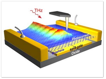
Researchers developed a technique for imaging THz photocurrents with nanoscale resolution, and applied it to visualize strongly compressed THz waves (plasmons) in a graphene photodetector. The extremely short wavelengths and highly concentrated fields of these plasmons open new venues for the development of miniaturized optoelectronic THz devices.
THz photocurrent nanoscopy of graphene plasmons in a split-gate photodetector
Radiation in the terahertz (THz) frequency range is attracting large interest because of its manifold application potential for non-destructive imaging, next-generation wireless communication or sensing. But still, the generating, detecting and controlling of THz radiation faces numerous technological challenges. Particularly, the relatively long wavelengths (from 30 to 300 mm) of THz radiation require solutions for nanoscale integration of THz devices or for nanoscale sensing and imaging applications.
In recent years, graphene plasmonics has become a highly promising platform for shrinking THz waves. It is based on the interaction of light with collective electron oscillations in graphene, giving rise to electromagnetic waves that are called plasmons. The graphene plasmons propagate with strongly reduced wavelength and can concentrate THz fields to subwavelength-scale dimensions, while the plasmons themselves can be controlled electrically.
Now, researchers at CIC nanoGUNE (San Sebastian, Spain) in collaboration with ICFO (Barcelona, Spain), IIT (Genova, Italy) - members of the EU Graphene Flagship - Columbia University (New York, USA), Radboud University (Nijmegen, Netherlands), NIM (Tsukuba, Japan) and Neaspec (Martinsried, Germany) could visualize strongly compressed and confined THz plasmons in a room-temperature THz detector based on graphene. To see the plasmons, they recorded a nanoscale map of the photocurrent that the detector produced while a sharp metal tip was scanned across it. The tip had the function to focus the THz illumination to a spot size of about 50 nm, which is about 2000 times smaller than the illumination wavelength. This new imaging technique, named THz photocurrent nanoscopy, provides unprecedented possibilities for characterizing optoelectronic properties at THz frequencies.
The team recorded photocurrent images of the graphene detector, while it was illuminated with THz radiation of around 100 mm wavelength. The images showed photocurrent oscillations revealing that THz plasmons with a more than 50 times reduced wavelength were propagating in the device while producing a photocurrent.
“In the beginning we were quite surprised about the extremely short plasmon wavelength, as THz graphene plasmons are typically much less compressed”, says former nanoGUNE researcher Pablo Alonso, now at the University of Oviedo, and first author of the work. “We managed to solve the puzzle by theoretical studies, which showed that the plasmons couple with the metal gate below the graphene”, he continues. “This coupling leads to an additional compression of the plasmons and an extreme field confinement, which could open the door towards various detector and sensor applications”, adds Rainer Hillenbrand, Ikerbasque Research Professor and Nanooptics Group Leader at nanoGUNE who led the research. The plasmons also show a linear dispersion – that means that their energy is proportional to their momentum - which could be beneficial for information and communication technologies. The team also analysed the lifetime of the THz plasmons, which showed that the damping of THz plasmons is determined by the impurities in the graphene.
THz photocurrent nanoscopy relies on the strong photothermoelectric effect in graphene, which transforms heat generated by THz fields, including that of THz plasmons, into a current. In the future, the strong thermoelectric effect could be also applied for on-chip THz plasmon detection in graphene plasmonic circuits. The technique for THz photocurrent nanoimaging could find further application potential beyond plasmon imaging, for example, for studying the local THz optoelectronic properties of other 2D materials, classical 2D electron gases or semiconductor nanostructures.
Share on:


Testimonial
"Advertising in PCB007 Magazine has been a great way to showcase our bare board testers to the right audience. The I-Connect007 team makes the process smooth and professional. We’re proud to be featured in such a trusted publication."
Klaus Koziol - atgSuggested Items
MEMS & Imaging Sensors Summit to Spotlight Sensing Revolution for Europe’s Leadership
09/11/2025 | SEMIIndustry experts will gather November 19-20 at the SEMI MEMS & Imaging Sensors Summit 2025 to explore the latest breakthroughs in AI-driven MEMS and imaging optimization, AR/VR technologies, and advanced sensor solutions for critical defence applications.
Direct Imaging System Market Size to Hit $4.30B by 2032, Driven by Increasing Demand for High-Precision PCB Manufacturing
09/11/2025 | Globe NewswireAccording to the SNS Insider, “The Direct Imaging System Market size was valued at $2.21 Billion in 2024 and is projected to reach $4.30 Billion by 2032, growing at a CAGR of 8.68% during 2025-2032.”
I-Connect007’s Editor’s Choice: Five Must-Reads for the Week
07/04/2025 | Marcy LaRont, I-Connect007For our industry, we have seen several bullish market announcements over the past few weeks, including one this week by IDC on the massive growth in the global server market. We’re also closely watching global trade and nearshoring. One good example of successful nearshoring is Rehm Thermal Systems, which celebrates its 10th anniversary in Mexico and the official opening of its new building in Guadalajara.
Driving Innovation: Direct Imaging vs. Conventional Exposure
07/01/2025 | Simon Khesin -- Column: Driving InnovationMy first camera used Kodak film. I even experimented with developing photos in the bathroom, though I usually dropped the film off at a Kodak center and received the prints two weeks later, only to discover that some images were out of focus or poorly framed. Today, every smartphone contains a high-quality camera capable of producing stunning images instantly.
United Electronics Corporation Advances Manufacturing Capabilities with Schmoll MDI-ST Imaging Equipment
06/24/2025 | United Electronics CorporationUnited Electronics Corporation has successfully installed the advanced Schmoll MDI-ST (XL) imaging equipment at their advanced printed circuit board facility. This significant technology investment represents a continued commitment to delivering superior products and maintaining their position as an industry leader in precision PCB manufacturing.