


 The Marketing Minute: Cracking the Code of Technical Marketing
 Trouble in Your Tank: Implementing Direct Metallization in Advanced Substrate Packaging


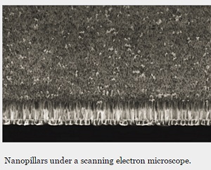
Nanopillars – A State-of-the-art Optical Sensor
November 8, 2016 | DTUEstimated reading time: 2 minutes
Reliable, cheap and quick recognition of molecules at challenging concentrations of ~1 ppb (parts per billion) or less is now possible thanks to a sensor developed at DTU Nanotech.
Potential analytes include toxic food additives, chemical warfare agents, hazardous building materials and human disease markers.
The sensor consists of nanopillars with heights of 600 – 800 nm. These pillars are able to enhance significantly the spectroscopic fingerprints of the target molecules nearby, making them distinguishable at ultra-low concentrations. The technique is called surface-enhanced Raman spectroscopy (SERS).
Postdoc Kaiyu Wu from DTU Nanotech says that “an ideal sensor for SERS should exhibit reproducibly high enhancement over macroscopic areas and be cost effective. It is extremely difficult to fulfil both.”
The nanopillar sensor is among the very few throughout the world known to achieve both standards.
Just like ‘pixels’
“Hot spots are the key elements in a SERS sensor, as they resolve the spectroscopic fingerprints of the target molecules. They are like pixels in a display that resolve different parts of an image. However, hot spots cannot be seen with the naked eye since their dimensions are only several to tens of nanometers”, says Kaiyu Wu.
The initial nanofabrication process of the nanopillar sensors was developed by Senior Researcher Michael Stenbæk Schmidt at DTU Nanotech. The process does not require any lengthy and expensive lithographic steps, thus it provides possibilities for the produced nanopillars to be used as cheap and expendable consumables.
The aim of Kaiyu Wu’s PhD project, which finished recently in June 2016, was to engineer ‘pixels’, i.e. hot spots in the nanopillars in order to take their sensing performance to the next level. This goal was achieved with the help of advanced spectroscopic and theoretical tools, as well as state-of-the-art nanofabrication techniques at DTU Nanotech and DTU Danchip.
The improved sensors now possess high-quality, high-density and reproducible nanoscale hot spots over macroscopic areas, as well as enhancement factors ultimately eclipsing the 100 million mark for molecular fingerprints.
The nanopillar sensors can be easily paired with portable read-out systems to enable on-site detection of analytes. Furthermore, their high-quality and high-density hot spots guarantee an extra-high sensitivity which reduces the time of detection to just several seconds for regular targets.
Kaiyu Wu’s research is part of the ‘NAPLAS – NAnoPLAsmonic Sensors’ project funded by The Danish Council for Independent Research, and the ‘HERMES – High Exponential Rise in Miniaturized cantilever-like Sensing’ project funded by the European Research Council.
Share on:


Testimonial
"In a year when every marketing dollar mattered, I chose to keep I-Connect007 in our 2025 plan. Their commitment to high-quality, insightful content aligns with Koh Young’s values and helps readers navigate a changing industry. "
Brent Fischthal - Koh YoungSuggested Items
PC Graphics Add-in Board Shipments Up 27% QoQ in 2Q25
09/03/2025 | Jon Peddie ResearchAccording to a new research report from the analyst firm Jon Peddie Research, the growth of the global PC-based graphics add-in board market reached 11.6 million units in Q2'25 and desktop PC CPUs shipments increased to 21.7 million units.
PC GPU Shipments Up 8.4% in 2Q25 on Pre-Tariff Demand
09/02/2025 | Jon Peddie ResearchJon Peddie Research reports the growth of the global PC-based graphics processor unit (GPU) market reached 74.7 million units in Q2'25, and PC CPU shipments increased to 66.9 million units.
20 Years of Center Nanoelectronic Technologies (CNT) – Backbone of German Semiconductor Research Celebrates Anniversary
08/14/2025 | Fraunhofer IPMSThe Center Nanoelectronic Technologies (CNT) of the Fraunhofer Institute for Photonic Microsystems (IPMS) is celebrating its 20th anniversary this year. Since its founding in 2005, it has developed into a pillar of applied semiconductor research in Germany and Europe. With its unique research cleanroom and equipment adhering to the 300-mm wafer industry standard, CNT is unparalleled in Germany and serves as a central innovation driver for the microelectronics industry.
Q2 Client CPU Shipments Increased 8% from Last Quarter, Up 13% YoY
08/13/2025 | Jon Peddie ResearchJon Peddie Research reports that the global client CPU market expanded for two quarters in a row, and in Q2’25, it showed unseasonal growth of 7.9% from last quarter, while server CPU shipments increased 22% year over year.
FuriosaAI Closes $125M Investment Round to Scale Production of Next-Gen AI Inference Chip
07/31/2025 | BUSINESS WIREFuriosaAI, a semiconductor company building a new foundation for AI compute, today announced it has completed a $125 million Series C bridge funding round. The investment continues a period of significant momentum for Furiosa as global demand for high-performance, efficient AI infrastructure soars.