


 The Marketing Minute: Cracking the Code of Technical Marketing
 Trouble in Your Tank: Implementing Direct Metallization in Advanced Substrate Packaging


Semiconductor-free Microelectronics Are Now Possible, Thanks to Metamaterials
November 8, 2016 | University of California - San DiegoEstimated reading time: 2 minutes
Engineers at the University of California San Diego have fabricated the first semiconductor-free, optically-controlled microelectronic device. Using metamaterials, engineers were able to build a microscale device that shows a 1,000 percent increase in conductivity when activated by low voltage and a low power laser.
The discovery paves the way for microelectronic devices that are faster and capable of handling more power, and could also lead to more efficient solar panels. The work was published in Nature Communications ("Photoemission-based microelectronic devices").
The capabilities of existing microelectronic devices, such as transistors, are ultimately limited by the properties of their constituent materials, such as their semiconductors, researchers said.
For example, semiconductors can impose limits on a device's conductivity, or electron flow. Semiconductors have what's called a band gap, meaning they require a boost of external energy to get electrons to flow through them. And electron velocity is limited, since electrons are constantly colliding with atoms as they flow through the semiconductor.
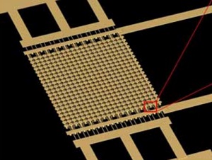
The designed semiconductor-free microelectronic device. (Image: UC San Diego Applied Electromagnetics Group)
A team of researchers in the Applied Electromagnetics Group led by electrical engineering professor Dan Sievenpiper at UC San Diego sought to remove these roadblocks to conductivity by replacing semiconductors with free electrons in space. "And we wanted to do this at the microscale," said Ebrahim Forati, a former postdoctoral researcher in Sievenpiper's lab and first author of the study.
Scanning electron micrograph images of the semiconductor-free microelectronic device (top left) and the gold metasurface (top right, bottom). (Image: UC San Diego Applied Electromagnetics Group)
However, liberating electrons from materials is challenging. It either requires applying high voltages (at least 100 Volts), high power lasers or extremely high temperatures (more than 1,000 degrees Fahrenheit), which aren't practical in micro- and nanoscale electronic devices.
To address this challenge, Sievenpiper's team fabricated a microscale device that can release electrons from a material without such extreme requirements. The device consists of an engineered surface, called a metasurface, on top of a silicon wafer, with a layer of silicon dioxide in between. The metasurface consists of an array of gold mushroom-like nanostructures on an array of parallel gold strips.
The gold metasurface is designed such that when a low DC voltage (under 10 Volts) and a low power infrared laser are both applied, the metasurface generates "hot spots"--spots with a high intensity electric field--that provide enough energy to pull electrons out from the metal and liberate them into space.
Tests on the device showed a 1,000 percent change in conductivity. "That means more available electrons for manipulation," Ebrahim said.
"This certainly won't replace all semiconductor devices, but it may be the best approach for certain specialty applications, such as very high frequencies or high power devices," Sievenpiper said.
According to researchers, this particular metasurface was designed as a proof-of-concept. Different metasurfaces will need to be designed and optimized for different types of microelectronic devices.
"Next we need to understand how far these devices can be scaled and the limits of their performance," Sievenpiper said. The team is also exploring other applications for this technology besides electronics, such as photochemistry, photocatalysis, enabling new kinds of photovoltaic devices or environmental applications.
Share on:


Testimonial
"The I-Connect007 team is outstanding—kind, responsive, and a true marketing partner. Their design team created fresh, eye-catching ads, and their editorial support polished our content to let our brand shine. Thank you all! "
Sweeney Ng - CEE PCBSuggested Items
Meet the Author Podcast: Martyn Gaudion Unpacks the Secrets of High-Speed PCB Design
07/16/2025 | I-Connect007In this special Meet the Author episode of the On the Line with… podcast, Nolan Johnson sits down with Martyn Gaudion, signal integrity expert, managing director of Polar Instruments, and three-time author in I-Connect007’s popular The Printed Circuit Designer’s Guide to... series.
Intervala Hosts Employee Car and Motorcycle Show, Benefit Nonprofits
08/27/2024 | IntervalaIntervala hosted an employee car and motorcycle show, aptly named the Vala-Cruise and it was a roaring success! Employees had the chance to show off their prized wheels, and it was incredible to see the variety and passion on display.
KIC Honored with IPC Recognition for 25 Years of Membership and Contributions to Electronics Manufacturing Industry
06/24/2024 | KICKIC, a renowned pioneer in thermal process and temperature measurement solutions for electronics manufacturing, is proud to announce that it has been recognized by IPC for 25 years of membership and significant contributions to electronics manufacturing.
Boeing Starliner Spacecraft Completes Successful Crewed Docking with International Space Station
06/07/2024 | BoeingNASA astronauts Barry "Butch" Wilmore and Sunita "Suni" Williams successfully docked Boeing's Starliner spacecraft to the International Space Station (ISS), about 26 hours after launching from Cape Canaveral Space Force Station.
KIC’s Miles Moreau to Present Profiling Basics and Best Practices at SMTA Wisconsin Chapter PCBA Profile Workshop
01/25/2024 | KICKIC, a renowned pioneer in thermal process and temperature measurement solutions for electronics manufacturing, announces that Miles Moreau, General Manager, will be a featured speaker at the SMTA Wisconsin Chapter In-Person PCBA Profile Workshop.