


 The Marketing Minute: Cracking the Code of Technical Marketing
 Trouble in Your Tank: Implementing Direct Metallization in Advanced Substrate Packaging


Silicon Photonics Industry Is Ready for Take-Off
November 9, 2016 | Yole DéveloppementEstimated reading time: 3 minutes
Datacenters with few other emerging applications will become a multibillion dollar market for silicon photonics by 2025. Transporting high level of data with existing technologies will soon reach its limit and photons will continue replacing step by step electrons throughout networks. Growing investments made by VCs have been identified by Yole Développements’ analysts and few startups have been created in this sector. All these indicators confirm the trend: silicon photonic technologies have reached the tipping point that precedes massive growth…
Yole Développement (Yole), the « More than Moore » market research and strategy consulting company releases this month the technology & market analysis titled Silicon Photonics for datacenters and other applications. Both experts Dr Eric Mounier, Sr Technnology & Market Analyst at Yole and Jean-Louis Malinge, former CEO of Kotura, now at ARCH Venture Partners combined their knowledge of the silicon photonic industry to perform a deep added-value analysis. Under this report, they examine the current status and future challenges for silicon photonics and data centers application. They detail for all applications, silicon photonic benefits as well as a comprehensive analysis of the industrial supply chain with player’s status.
What is the status of silicon photonic technologies? Could we already speak about commercial solutions? What is the market size today? What about tomorrow? How high are the current investments?... Yole’s analysts offer you a snapshot of the story.
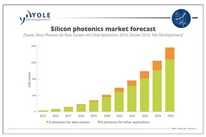
The silicon photonics market is still modest with estimated sales below US$40 million in 2015 and very few companies actually shipping products in the open market: Mellanox, Cisco, Luxtera, Intel, STMicroelectronics, Acacia and Molex are part of these leading players.
Silicon photonics has been under development for years. However now, this technology is being pushed hard by large webcom companies like Facebook and Microsoft. “Silicon photonics has reached the tipping point that precedes massive growth”, comments Dr Eric Mounier from Yole. “Indeed we estimate, the packaged silicon photonics transceiver market will be worth US$6 billion in 10 years.”
Silicon photonics is an exciting technology mixing optics, CMOS technology and advanced packaging. This combination benefits from semiconductor wafer manufacturing scalability to reduce costs.
“Silicon photonics offers silicon technology advantages including higher integration, more functionalities embedded with lower power consumption and better reliability compared to legacy optics”, analyzes Jean-Louis Malinge.
In 2020 and more, silicon photonic chips will far exceed copper cabling capabilities. Such solutions will be so deployed in high-speed signal transmission systems. In 2025 and more, the technology will be more and more used in processing such as interconnecting multiple cores with processor chips. Indeed, according to Yole’s analysts, the chip market value should score US$1,5 billion in 2025 at chip level (Estimated to be less than US$40 million in 2015). Step by step photons get closer to the chips!
Data centers are clearly the best opportunity for silicon photonics technology today. And there are also many other applications that silicon photonics can enable. These include high performance computers, telecommunications, sensors, life science, quantum computers and other high-end applications.
Two applications are particularly interesting as silicon photonics can push the integration of optical functions and miniaturization further to achieve successful products. Those applications are lidars for autonomous cars and biochemical and chemical sensors.
Lidars are costly and bulky instruments which make their integration in a car challenging. Within a promising ADAS market expected to reach US$3,9 billion in 2017 silicon photonic-based lidar will play a key role. Indeed silicon photonics allow lidar without moving elements, which can experience issues in a harsh car environment. Last august, MIT’s Photonic Microsystems Group announced a successful DARPA project using silicon photonics for lidar-on-a-chip with steerable transmitting and receiving phased arrays and on-chip Ge photodetectors.
Biochemical and gas sensors are not new, and several applications have existed for a while. Day by day, the interest in gas sensing is gaining importance due to the emergence of promising new large volume portable applications. Integration of biochemical or gas sensors into smartphones or wearables is currently on the roadmap of many companies but size, cost and sensitivity are still issues. To push optical gas sensor miniaturization further, some companies are already considering silicon photonics as an integration platform for their devices.
Share on:


Testimonial
"We’re proud to call I-Connect007 a trusted partner. Their innovative approach and industry insight made our podcast collaboration a success by connecting us with the right audience and delivering real results."
Julia McCaffrey - NCAB GroupSuggested Items
Trouble in Your Tank: Implementing Direct Metallization in Advanced Substrate Packaging
09/15/2025 | Michael Carano -- Column: Trouble in Your TankDirect metallization systems based on conductive graphite are gaining popularity throughout the world. The environmental and productivity gains achievable with this process are outstanding. Direct metallization reduces the costs of compliance, waste treatment, and legal issues related to chemical exposure. A graphite-based direct plate system has been devised to address these needs.
Closing the Loop on PCB Etching Waste
09/09/2025 | Shawn Stone, IECAs the PCB industry continues its push toward greener, more cost-efficient operations, Sigma Engineering’s Mecer System offers a comprehensive solution to two of the industry’s most persistent pain points: etchant consumption and rinse water waste. Designed as a modular, fully automated platform, the Mecer System regenerates spent copper etchants—both alkaline and acidic—and simultaneously recycles rinse water, transforming a traditionally linear chemical process into a closed-loop system.
Driving Innovation: Depth Routing Processes—Achieving Unparalleled Precision in Complex PCBs
09/08/2025 | Kurt Palmer -- Column: Driving InnovationIn PCB manufacturing, the demand for increasingly complex and miniaturized designs continually pushes the boundaries of traditional fabrication methods, including depth routing. Success in these applications demands not only on robust machinery but also sophisticated control functions. PCB manufacturers rely on advanced machine features and process methodologies to meet their precise depth routing goals. Here, I’ll explore some crucial functions that empower manufacturers to master complex depth routing challenges.
Trouble in Your Tank: Minimizing Small-via Defects for High-reliability PCBs
08/27/2025 | Michael Carano -- Column: Trouble in Your TankTo quote the comedian Stephen Wright, “If at first you don’t succeed, then skydiving is not for you.” That can be the battle cry when you find that only small-diameter vias are exhibiting voids. Why are small holes more prone to voids than larger vias when processed through electroless copper? There are several reasons.
The Government Circuit: Navigating New Trade Headwinds and New Partnerships
08/25/2025 | Chris Mitchell -- Column: The Government CircuitAs global trade winds continue to howl, the electronics manufacturing industry finds itself at a critical juncture. After months of warnings, the U.S. Government has implemented a broad array of tariff increases, with fresh duties hitting copper-based products, semiconductors, and imports from many nations. On the positive side, tentative trade agreements with Europe, China, Japan, and other nations are providing at least some clarity and counterbalance.