


 The Marketing Minute: Cracking the Code of Technical Marketing
 Trouble in Your Tank: Implementing Direct Metallization in Advanced Substrate Packaging


New 'Bottlebrush' Electroactive Polymers Make Dielectric Elastomers Increasingly Viable for Use in Devices
November 9, 2016 | North Carolina State UniversityEstimated reading time: 2 minutes
A multi-institutional research team has developed a new electroactive polymer material that can change shape and size when exposed to a relatively small electric field. The advance overcomes two longstanding challenges regarding the use of electroactive polymers to develop new devices, opening the door to a suite of applications ranging from microrobotics to designer haptic, optic, microfluidic and wearable technologies. The work was performed by researchers at North Carolina State University, the University of North Carolina at Chapel Hill, Carnegie Mellon University and the University of Akron.
“Dielectric elastomers are the most responsive electroactive polymers in terms of achievable strains, but two big hurdles have effectively prevented the smart materials community from using them in commercial devices,” says Richard J. Spontak, Distinguished Professor of Chemical and Biomolecular Engineering and professor of materials science and engineering at NC State, who co-authored a paper describing the new materials. “First, previous dielectric elastomers required large electric fields in order to trigger actuation, or movement – on the order of at least 100 kilovolts per millimeter (kV/mm). With our new material, we can see actuation at levels as low as ca. 10 kV/mm.”
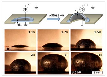
Electrical response of a circular diaphragm composed of a pure bottlebrush elastomer upon electroactuation with increasing voltage and without any external pre-strain. The numbers indicate the electric field-induced area expansion under constant-volume conditions at room temperature. (click on image to enlarge)
“The second challenge is that, previously, materials had to be pre-strained,” Spontak says. “This would either mean using a frame to physically strain the material, or adding a second component to the polymer to retain the strain after it was applied. But our material consists of a single component that is specifically designed at the molecular level to inherently possess pre-strain. In other words, we don’t need a frame or a second component – our material is ready to be used as soon as it is cross-linked into a specific shape.”
The new material that has permitted this breakthrough is a “bottlebrush” silicone elastomer, which has been engineered to possess these unique properties, and it is not difficult to manufacture.
“We are working specifically with bottlebrush polymers, which are prepared by grafting long polymeric side chains to a polymer backbone,” says Sergei S. Sheiko, George A. Bush, Jr. Distinguished Professor of Chemistry at UNC and corresponding author of the paper (Advanced Materials, "Bottlebrush Elastomers: A New Platform for Freestanding Electroactuation"). “The resulting molecules may be viewed as filaments that are thick, yet remain quite flexible, which allows for significant reduction of the materials’ rigidity and makes them more stretchable. Furthermore, the mechanical properties can be controlled by varying the bottlebrush architecture – for example, by preparing molecules with different degrees of polymerization of grafted chains and different grafting densities.
“This architectural control of mechanical properties has reduced the limit of stiffness in dry polymer materials by 1,000 times, demonstrated extensibility of up to eight times, and opened up new applications not available to stiffer materials or materials with liquid fractions,” Sheiko says. “One of these applications – their use as free-standing dielectric elastomers – has been demonstrated, which we discuss in this paper.”
“We’re at the earliest stages of identifying all the potential ways in which we could use this new class of material,” Spontak says. “It works better than anticipated, and now we’re beginning to consider potential applications.”
This video shows reversible electrical actuation of a pure bottlebrush elastomer without the addition of any external pre-strain (which, trust us, is pretty interesting if you're an engineer).
Share on:


Testimonial
"In a year when every marketing dollar mattered, I chose to keep I-Connect007 in our 2025 plan. Their commitment to high-quality, insightful content aligns with Koh Young’s values and helps readers navigate a changing industry. "
Brent Fischthal - Koh YoungSuggested Items
Curing and Verification in PCB Shadow Areas
09/17/2025 | Doug Katze, DymaxDesign engineers know a simple truth that often complicates electronics manufacturing: Light doesn’t go around corners. In densely populated PCBs, adhesives and coatings often fail to fully cure in shadowed regions created by tall ICs, connectors, relays, and tight housings.
Marcy’s Musings: Advancing the Advanced Materials Discussion
09/17/2025 | Marcy LaRont -- Column: Marcy's MusingsAs the industry’s most trusted global source of original content about the electronics supply chain, we continually ask you about your concerns, what you care about, and what you most want to learn about. Your responses are insightful and valuable. Thank you for caring enough to provide useful feedback and engage in dialogue.
September 2025 PCB007 Magazine: The Future of Advanced Materials
09/16/2025 | I-Connect007 Editorial TeamMoore’s Law is no more, and the advanced material solutions being developed to grapple with this reality are surprising, stunning, and perhaps a bit daunting. Buckle up for a dive into advanced materials and a glimpse into the next chapters of electronics manufacturing.
I-Connect007 Launches Advanced Electronics Packaging Digest
09/15/2025 | I-Connect007I-Connect007 is pleased to announce the launch of Advanced Electronics Packaging Digest (AEPD), a new monthly digital newsletter dedicated to one of the most critical and rapidly evolving areas of electronics manufacturing: advanced packaging at the interconnect level.
Panasonic Industry will Double the Production Capacity of MEGTRON Multi-layer Circuit Board Materials Over the Next Five Years
09/15/2025 | Panasonic Industry Co., Ltd.Panasonic Industry Co., Ltd., a Panasonic Group company, announced plans for a major expansion of its global production capacity for MEGTRON multi-layer circuit board materials today. The company plans to double its production over the next five years to meet growing demand in the AI server and ICT infrastructure markets.