


 The Marketing Minute: Cracking the Code of Technical Marketing
 Trouble in Your Tank: Implementing Direct Metallization in Advanced Substrate Packaging


Solar Cells Get Boost With Integration of Water-Splitting Catalyst Onto Semiconductor
November 10, 2016 | Lawrence Berkeley National LaboratoryEstimated reading time: 3 minutes
Scientists have found a way to engineer the atomic-scale chemical properties of a water-splitting catalyst for integration with a solar cell, and the result is a big boost to the stability and efficiency of artificial photosynthesis.
Led by researchers at the Department of Energy’s Lawrence Berkeley National Laboratory (Berkeley Lab), the project is described in a paper published this week in the journal Nature Materials ("A multifunctional biphasic water splitting catalyst tailored for integration with high-performance semiconductor photoanodes").
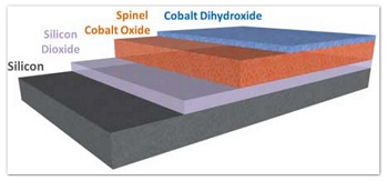
Schematic of the multi-functional water splitting catalyst layer engineered using atomic layer deposition for integration with a high-efficiency silicon cell. (Image: Ian Sharp/Berkeley Lab)
The research comes out of the Joint Center for Artificial Photosynthesis (JCAP), a DOE Energy Innovation Hub established in 2010 to develop a cost-effective method of turning sunlight, water, and carbon dioxide into fuel. JCAP is led by the California Institute of Technology with Berkeley Lab as a major partner.
The goal of this study was to strike a careful balance between the contradictory needs for efficient energy conversion and chemically sensitive electronic components to develop a viable system of artificial photosynthesis to generate clean fuel.
Striking the right balance
“In order for an artificial photosystem to be viable, we need to be able to make it once, deploy it, and have it last for 20 or more years without repairing it,” said study principal investigator Ian Sharp, head of materials integration and interface science research at JCAP.
The problem is that the active chemical environments needed for artificial photosynthesis are damaging to the semiconductors used to capture solar energy and power the device.
“Good protection layers are dense and chemically inactive. That is completely at odds with the characteristics of an efficient catalyst, which helps to split water to store the energy of light in chemical bonds,” said Sharp, who is also a staff scientist at Berkeley Lab’s Chemical Sciences Division. “The most efficient catalysts tend to be permeable and easily transform from one phase to another. These types of materials would usually be considered poor choices for protecting electronic components.”
By engineering an atomically precise film so that it can support chemical reactions without damaging sensitive semiconductors, the researchers managed to satisfy contradictory needs for artificial photosystems.
“This gets into the key aspects of our work,” said study lead author Jinhui Yang, who conducted the work as a postdoctoral researcher at JCAP. “We set out to turn the catalyst into a protective coating that balances these competing properties.”
Doing double duty
The researchers knew they needed a catalyst that could not only support active and efficient chemical reactions, but one that could also provide a stable interface with the semiconductor, allow the charge generated by the absorption of light from the semiconductor to be efficiently transferred to the sites doing catalysis, and permit as much light as possible to pass through.
They turned to a manufacturing technique called plasma-enhanced atomic layer deposition, performed at the Molecular Foundry at Berkeley Lab. This type of thin-film deposition is used in the semiconductor industry to manufacture integrated circuits.
“This technique gave us the level of precision we needed to create the composite film,” said Yang. “We were able to engineer a very thin layer to protect the sensitive semiconductor, then atomically join another active layer to carry out the catalytic reactions, all in a single process.”
The first layer of the film consisted of a nanocrystalline form of cobalt oxide that provided a stable, physically robust interface with the light-absorbing semiconductor. The other layer was a chemically reactive material made of cobalt dihydroxide.
“The design of this composite coating was inspired by recent advances in the field that have revealed how water-splitting reactions occur, at the atomic scale, on materials. In this way, mechanistic insights guide how to make systems that have the functional properties we need,” said Sharp.
Using this configuration, the researchers could run photosystems continuously for three days—potentially longer—when such systems would normally fail in mere seconds.
“A major impact of this work is to demonstrate the value of designing catalysts for integration with semiconductors,” said Yang. “Using a combination of spectroscopic and electrochemical methods, we showed that these films can be made compact and continuous at the nanometer scale, thus minimizing parasitic light absorption when integrated on top of photoactive semiconductors.”
The study authors noted that while this is an important milestone, there are many more steps needed before a commercially viable artificial photosystem is ready for deployment.
“In general, we need to know more about how these systems fail so we can identify areas to target for future improvement,” said Sharp. “Understanding degradation is an important avenue to making something that is stable for decades.”
Share on:


Testimonial
"We’re proud to call I-Connect007 a trusted partner. Their innovative approach and industry insight made our podcast collaboration a success by connecting us with the right audience and delivering real results."
Julia McCaffrey - NCAB GroupSuggested Items
Beyond Design: Slaying Signal Integrity Villains
09/17/2025 | Barry Olney -- Column: Beyond DesignHigh-speed PCB design is a balancing act, where subtle oversights can develop into major signal integrity nightmares. Some culprits lie dormant during early validation, only to reveal themselves later through workflow disruptions and elusive performance bottlenecks. Take crosstalk, for example. What begins as a stray signal coupling between traces can ripple through the design, ultimately destabilizing the power distribution network. Each of these troublemakers operates with signature tactics, but they also have well-known vulnerabilities.
Driving Innovation: Depth Routing Processes—Achieving Unparalleled Precision in Complex PCBs
09/08/2025 | Kurt Palmer -- Column: Driving InnovationIn PCB manufacturing, the demand for increasingly complex and miniaturized designs continually pushes the boundaries of traditional fabrication methods, including depth routing. Success in these applications demands not only on robust machinery but also sophisticated control functions. PCB manufacturers rely on advanced machine features and process methodologies to meet their precise depth routing goals. Here, I’ll explore some crucial functions that empower manufacturers to master complex depth routing challenges.
Global PCB Connections: Understanding the General Fabrication Process—A Designer’s Hidden Advantage
08/14/2025 | Markus Voeltz -- Column: Global PCB ConnectionsDesigners don’t need to become fabricators, but understanding the basics of PCB fabrication can save you time, money, and frustration. The more you understand what’s happening on the shop floor, the better you’ll be able to prevent downstream issues. As you move into more advanced designs like HDI, flex circuits, stacked vias, and embedded components, this foundational knowledge becomes even more critical. Remember: the fabricator is your partner.
I-Connect007 Editor’s Choice: Five Must-Reads for the Week
08/08/2025 | Andy Shaughnessy, I-Connect007If you’ve been watching the news lately, you might be tempted to opine, “What’s going on here?” In this week’s must-reads, we have a wrap-up of the latest news about U.S. tariffs with Asia, and columnist Tom Yang explains why some PCB fabrication business should remain in China. We also have a piece that examines the unprecedented growth that green manufacturing is expected to see over the next four years.
Driving Innovation: Inner Layer Alignment Methods in PCB Production
08/06/2025 | Kurt Palmer -- Column: Driving InnovationIn PCB manufacturing, precision is a fundamental requirement. Among many complex processes, the accurate registration of inner layers before lamination is one of the most critical. Much like a child's game where rings must be perfectly stacked onto a single pin, PCB manufacturers align multiple conductive and insulating layers to form a cohesive, functional board. This alignment directly affects PCB precision; tighter layer alignment results in smaller "annular rings," superior performance, and higher yields.