


 The Marketing Minute: Cracking the Code of Technical Marketing
 Trouble in Your Tank: Implementing Direct Metallization in Advanced Substrate Packaging


Nanoelectronics Scores Laboratory Victory
November 10, 2016 | New York UniversityEstimated reading time: 2 minutes
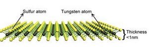
Researchers at the NYU Tandon School of Engineering have pioneered a method for growing an atomic scale electronic material at the highest quality ever reported. In a paper published in Applied Physics Letters ("Electronic Properties of Monolayer Tungsten Disulfide Grown by Chemical Vapor Deposition"), Assistant Professor of Electrical and Computer Engineering Davood Shahrjerdi and doctoral student Abdullah Alharbi detail a technique for synthesizing large sheets of high-performing monolayer tungsten disulfide, a synthetic material with a wide range of electronic and optoelectronic applications.
"We developed a custom reactor for growing this material using a routine technique called chemical vapor deposition. We made some subtle and yet critical changes to improve the design of the reactor and the growth process itself, and we were thrilled to discover that we could produce the highest quality monolayer tungsten disulfide reported in the literature," said Shahrjerdi. "It's a critical step toward enabling the kind of research necessary for developing next-generation transistors, wearable electronics, and even flexible biomedical devices."
At just one atom thick, tungsten disulfide allows energy to switch off and on -- important for nano-scale electronic transistors -- but it also absorbs and emits light, which could find applications in optoelectronics, sensing, and flexible electronics. The NYU logo shows the monolayer material emitting light. Researchers at NYU Tandon reported success in growing the promising monolayer material. (click on image to enlarge)
At just one atom thick, tungsten disulfide allows energy to switch off and on -- important for nano-scale electronic transistors -- but it also absorbs and emits light, which could find applications in optoelectronics, sensing, and flexible electronics. The NYU logo shows the monolayer material emitting light. Researchers at NYU Tandon reported success in growing the promising monolayer material.
The promise of two-dimensional electronic materials has tantalized researchers for more than a decade, since the first such material — graphene — was experimentally discovered. Also called "monolayer" materials, graphene and similar two-dimensional materials are a mere one atom in thickness, several hundred thousand times thinner than a sheet of paper. These materials boast major advantages over silicon — namely unmatched flexibility, strength, and conductivity — but developing practical applications for their use has been challenging.
Graphene (a single layer of carbon) has been explored for electronic switches (transistors), but its lack of an energy band gap poses difficulties for semiconductor applications. "You can't turn off the graphene transistors," explained Shahrjerdi. Unlike graphene, tungsten disulfide has a sizeable energy band gap. It also displays exciting new properties: When the number of atomic layers increases, the band gap becomes tunable, and at monolayer thickness it can strongly absorb and emit light, making it ideal for applications in optoelectronics, sensing, and flexible electronics.
Efforts to develop applications for monolayer materials are often plagued by imperfections in the material itself — impurities and structural disorders that can compromise the movement of charge carriers in the semiconductor (carrier mobility). Shahrjerdi and his student succeeded in reducing the structural disorders by omitting the growth promoters and using nitrogen as a carrier gas rather than a more common choice, argon.
Shahrjerdi noted that comprehensive testing of their material revealed the highest values recorded thus far for carrier mobility in monolayer tungsten disulfide. "It's a very exciting development for those of us doing research in this field," he said.
Share on:


Testimonial
"Our marketing partnership with I-Connect007 is already delivering. Just a day after our press release went live, we received a direct inquiry about our updated products!"
Rachael Temple - AlltematedSuggested Items
Curing and Verification in PCB Shadow Areas
09/17/2025 | Doug Katze, DymaxDesign engineers know a simple truth that often complicates electronics manufacturing: Light doesn’t go around corners. In densely populated PCBs, adhesives and coatings often fail to fully cure in shadowed regions created by tall ICs, connectors, relays, and tight housings.
Marcy’s Musings: Advancing the Advanced Materials Discussion
09/17/2025 | Marcy LaRont -- Column: Marcy's MusingsAs the industry’s most trusted global source of original content about the electronics supply chain, we continually ask you about your concerns, what you care about, and what you most want to learn about. Your responses are insightful and valuable. Thank you for caring enough to provide useful feedback and engage in dialogue.
September 2025 PCB007 Magazine: The Future of Advanced Materials
09/16/2025 | I-Connect007 Editorial TeamMoore’s Law is no more, and the advanced material solutions being developed to grapple with this reality are surprising, stunning, and perhaps a bit daunting. Buckle up for a dive into advanced materials and a glimpse into the next chapters of electronics manufacturing.
I-Connect007 Launches Advanced Electronics Packaging Digest
09/15/2025 | I-Connect007I-Connect007 is pleased to announce the launch of Advanced Electronics Packaging Digest (AEPD), a new monthly digital newsletter dedicated to one of the most critical and rapidly evolving areas of electronics manufacturing: advanced packaging at the interconnect level.
Panasonic Industry will Double the Production Capacity of MEGTRON Multi-layer Circuit Board Materials Over the Next Five Years
09/15/2025 | Panasonic Industry Co., Ltd.Panasonic Industry Co., Ltd., a Panasonic Group company, announced plans for a major expansion of its global production capacity for MEGTRON multi-layer circuit board materials today. The company plans to double its production over the next five years to meet growing demand in the AI server and ICT infrastructure markets.