


 The Marketing Minute: Cracking the Code of Technical Marketing
 Trouble in Your Tank: Implementing Direct Metallization in Advanced Substrate Packaging


Graphene Plasmons Reach the Infrared
November 15, 2016 | The Optical SocietyEstimated reading time: 3 minutes
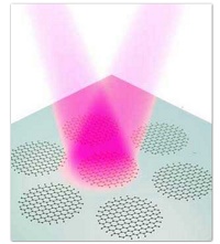
Graphene's unique properties can be both a blessing and a curse to researchers, especially to those at the intersection of optical and electronic applications. These single-atom thick sheets feature highly mobile electrons on their flexible profiles, making them excellent conductors, but in general graphene sheets do not interact with light efficiently.
Problematic for shorter wavelength light, photons in the near infrared region of the spectrum, where telecommunication applications become realizable. In a paper published this week in the journal Optics Letters ("Experimental demonstration of graphene plasmons working close to the near-infrared window"), from The Optical Society (OSA), researchers at the Technical University of Denmark have demonstrated, for the first time, efficient absorption enhancement at a wavelength of 2 micrometers by graphene, specifically by the plasmons of nanoscale graphene disks.
Graphene Plasmons Reach the Infrared
Much like water ripples arising from the energy of a dropped pebble, electronic oscillations can arise in freely moving conduction electrons by absorbing light energy. The resulting collective, coherent motions of these electrons are called plasmons, which also serve to amplify the strength of the absorbed light's electric field at close proximity. Plasmons are becoming increasingly commonplace in various optoelectronic applications where highly conductive metals can be easily integrated.
Graphene plasmons, however, face an extra set of challenges unfamiliar to the plasmons of bulk metals. One of these challenges is the relatively long wavelength needed to excite them. Many efforts taking advantage of the enhancing effects of plasmons on graphene have demonstrated promise, but for low energy light.
"The motivation of our work is to push graphene plasmons to shorter wavelengths in order to integrate graphene plasmon concepts with existing mature technologies," said Sanshui Xiao, associate professor from the Technical University of Denmark.
To do so, Xiao, Wang and their collaborators took inspiration from recent developments at the university's Center of Nanostructured Graphene (CNG), where they demonstrated a self-assembly method resulting in large arrays of graphene nanostructures. Their method primarily uses geometry to bolster the graphene plasmon effects at shorter wavelengths by decreasing the size of the graphene structures.
Using lithographic masks prepared by a block copolymer based self-assembly method, the researchers made arrays of graphene nanodisks. They controlled the final size of the disks by exposing the array to oxygen plasma which etched away at the disks, bringing the average diameter down to approximately 18 nm. This is approximately 1000 times smaller than the width of a human hair.
The array of approximately 18 nm disks, resulting from 10 seconds of etching with oxygen plasma, showed a clear resonance with 2 micrometer wavelength light, the shortest wavelength resonance ever observed in graphene plasmons.
An assumption might be that longer etching times or finer lithographic masks, and therefore smaller disks, would result in even shorter wavelengths. Generally speaking this is true, but at 18 nm the disks already start requiring consideration of atomic details and quantum effects.
Instead, the team plans to tune graphene plasmon resonances at smaller scales in the future using electrical gating methods, where the local concentration of electrons and electric field profile alter resonances.
Xiao said, "To further push graphene plasmons to shorter wavelengths, we plan to use electrical gating. Instead of graphene disks, graphene antidots (i.e. graphene sheets with regular holes) will be chosen because it is easy to implement a back-gating technique."
There are also fundamental limits to the physics that prevent shortening the graphene plasmon resonance wavelength with more etching. "When the wavelength becomes shorter, the interband transition will soon play a key role, leading to broadening of the resonance. Due to weak coupling of light with graphene plasmons and this broadening effect, it will become hard to observe the resonance feature," Xiao explained.
Share on:


Testimonial
"The I-Connect007 team is outstanding—kind, responsive, and a true marketing partner. Their design team created fresh, eye-catching ads, and their editorial support polished our content to let our brand shine. Thank you all! "
Sweeney Ng - CEE PCBSuggested Items
Closing the Loop on PCB Etching Waste
09/09/2025 | Shawn Stone, IECAs the PCB industry continues its push toward greener, more cost-efficient operations, Sigma Engineering’s Mecer System offers a comprehensive solution to two of the industry’s most persistent pain points: etchant consumption and rinse water waste. Designed as a modular, fully automated platform, the Mecer System regenerates spent copper etchants—both alkaline and acidic—and simultaneously recycles rinse water, transforming a traditionally linear chemical process into a closed-loop system.
The Chemical Connection: Through-glass Vias in Glass Substrates
06/24/2025 | Don Ball -- Column: The Chemical ConnectionThis month’s theme is vias and how best to ensure via quality and reliability. I don’t have much expertise in this process area or much to contribute that most of you don’t already know. However, I’ve recently become peripherally involved in a via technology that may be of more than academic interest to some of us. It entails putting vias in a material not usually associated with PCB manufacturing: through-glass vias (TGVs) in glass substrates.
In Pursuit of Perfection: Defect Reduction—May 2025 PCB007 Magazine Now Available
05/15/2025 | I-Connect007 Editorial TeamFor bare PCB board fabrication, defect reduction is a critical aspect of a company's bottom line profitability. In the May 2025 issue of PCB007 Magazine, we examine the imaging, etching, and plating processes, as well as product traceability on the shop floor, providing information and insight into how you can reduce your defects and increase yields.
DuPont to Showcase Advanced Semiconductor Wet Etching Innovations at the Surface Preparation and Cleaning Conference
05/13/2025 | DuPontDuPont announced that it will present its latest developments in semiconductor wet etching technologies at the upcoming Surface Preparation and Cleaning Conference (SPCC) in Chandler, Arizona, beginning May 20.
The Chemical Connection: Common Misconceptions in Wet Processing
04/28/2025 | Don Ball -- Column: The Chemical ConnectionInitially, I thought an April Fool’s column would be fun this month. I could highlight some of the crazier ideas and misconceptions I’ve witnessed over the years from potential customers and we could all have a good laugh. For example, there was a first-time buyer of a ferric chloride etcher (with no regeneration system) who was astonished to learn that he had to put fresh etchant in the system occasionally to maintain production.