


 The Marketing Minute: Cracking the Code of Technical Marketing
 Trouble in Your Tank: Implementing Direct Metallization in Advanced Substrate Packaging


A New Way to Image Solar Cells in 3-D
November 16, 2016 | LBLEstimated reading time: 3 minutes
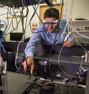
Next-generation solar cells made of super-thin films of semiconducting material hold promise because they’re relatively inexpensive and flexible enough to be applied just about anywhere.
Researchers are working to dramatically increase the efficiency at which thin-film solar cells convert sunlight to electricity. But it’s a tough challenge, partly because a solar cell’s subsurface realm—where much of the energy-conversion action happens—is inaccessible to real-time, nondestructive imaging. It’s difficult to improve processes you can’t see.
Now, scientists from the Department of Energy’s Lawrence Berkeley National Laboratory (Berkeley Lab) have developed a way to use optical microscopy to map thin-film solar cells in 3-D as they absorb photons.
The method, reported Nov. 15 in the journal Advanced Materials, was developed at the Molecular Foundry, a DOE Office of Science user facility located at Berkeley Lab. It images optoelectronic dynamics in materials at the micron scale, or much thinner than the diameter of a human hair. This is small enough to see individual grain boundaries, substrate interfaces, and other internal obstacles that can trap excited electrons and prevent them from reaching an electrode, which saps a solar cell’s efficiency.
So far, scientists have used the technique to better understand why adding a specific chemical to solar cells made of cadmium telluride (CdTe)—the most common thin-film material—improves the solar cells’ performance.
“To make big gains in photovoltaic efficiency, we need to see what’s happening throughout a working photovoltaic material at the micron scale, both on the surface and below, and our new approach allows us to do that,” says Edward Barnard, a principal scientific engineering associate at the Molecular Foundry. He led the effort with James Schuck, the director of the Imaging and Manipulation of Nanostructures facility at the Molecular Foundry.
The imaging method is born out of a collaboration between Molecular Foundry scientists and Foundry users from PLANT PV Inc., an Alameda, California-based company. While fabricating new solar cell materials at the Molecular Foundry, the team found that standard optical techniques couldn’t image the inner-workings of the materials, so they developed the new technique to obtain this view. Next, scientists from the National Renewable Energy Laboratory came to the Molecular Foundry and used the new method to study CdTe solar cells.
To develop the approach, the scientists modified a technique called two-photon microscopy (which is used by biologists to see inside thick samples such as living tissue) so that it can be applied to bulk semiconductor materials.
The method uses a highly focused laser beam of infrared photons that penetrate inside the photovoltaic material. When two low-energy photons converge at the same pinpoint, there’s enough energy to excite electrons. These electrons can be tracked to see how long they last in their excited state, with long-lifetime electrons appearing as bright spots in microscopy images. In a solar cell, long-lifetime electrons are more likely to reach an electrode.
In addition, the laser beam can be systematically repositioned throughout a test-sized solar cell, creating a 3-D map of a solar cell’s entire optoelectronic dynamics.
The method has already shed light on the benefits of treating CdTe solar cells with cadmium chloride, which is often added during the fabrication process.
Scientists know cadmium chloride improves the efficiency of CdTe solar cells, but its effect on excited electrons at the micron scale is not well understood. Studies have shown that the chlorine ions tend to pile up at grain boundaries, but how this changes the lifetime of excited electrons is unclear.
Thanks to the new imaging technique, the researchers discovered the cadmium chloride treatment increases the lifetime of excited electrons at the grain boundaries, as well as within the grains themselves. This is easily seen in 3-D images of CdTe solar cells with and without the treatment. The treated solar cell “lights up” much more uniformly throughout the material, both in the grains and the spaces in between.
“Scientists have known that cadmium chloride passivation improves the lifetime of electrons in CdTe cells, but now we’ve mapped at the micron scale where this improvement occurs,” says Barnard.
The new imaging technique could help scientists make more informed decisions about improving a host of thin-film solar cell materials in addition to CdTe, such as perovskite and organic compounds.
“Researchers trying to push photovoltaic efficiency could use our technique to see if their strategies are working at the microscale, which will help them design better test-scale solar cells—and eventually full-sized solar cells for rooftops and other real-world applications,” he says.
The research was supported by the Department of Energy’s Office of Science and by a SunShot Initiative award from the Office of Energy Efficiency and Renewable Energy.
Share on:


Testimonial
"The I-Connect007 team is outstanding—kind, responsive, and a true marketing partner. Their design team created fresh, eye-catching ads, and their editorial support polished our content to let our brand shine. Thank you all! "
Sweeney Ng - CEE PCBSuggested Items
MEMS & Imaging Sensors Summit to Spotlight Sensing Revolution for Europe’s Leadership
09/11/2025 | SEMIIndustry experts will gather November 19-20 at the SEMI MEMS & Imaging Sensors Summit 2025 to explore the latest breakthroughs in AI-driven MEMS and imaging optimization, AR/VR technologies, and advanced sensor solutions for critical defence applications.
Direct Imaging System Market Size to Hit $4.30B by 2032, Driven by Increasing Demand for High-Precision PCB Manufacturing
09/11/2025 | Globe NewswireAccording to the SNS Insider, “The Direct Imaging System Market size was valued at $2.21 Billion in 2024 and is projected to reach $4.30 Billion by 2032, growing at a CAGR of 8.68% during 2025-2032.”
I-Connect007’s Editor’s Choice: Five Must-Reads for the Week
07/04/2025 | Marcy LaRont, I-Connect007For our industry, we have seen several bullish market announcements over the past few weeks, including one this week by IDC on the massive growth in the global server market. We’re also closely watching global trade and nearshoring. One good example of successful nearshoring is Rehm Thermal Systems, which celebrates its 10th anniversary in Mexico and the official opening of its new building in Guadalajara.
Driving Innovation: Direct Imaging vs. Conventional Exposure
07/01/2025 | Simon Khesin -- Column: Driving InnovationMy first camera used Kodak film. I even experimented with developing photos in the bathroom, though I usually dropped the film off at a Kodak center and received the prints two weeks later, only to discover that some images were out of focus or poorly framed. Today, every smartphone contains a high-quality camera capable of producing stunning images instantly.
United Electronics Corporation Advances Manufacturing Capabilities with Schmoll MDI-ST Imaging Equipment
06/24/2025 | United Electronics CorporationUnited Electronics Corporation has successfully installed the advanced Schmoll MDI-ST (XL) imaging equipment at their advanced printed circuit board facility. This significant technology investment represents a continued commitment to delivering superior products and maintaining their position as an industry leader in precision PCB manufacturing.