


 The Marketing Minute: Cracking the Code of Technical Marketing
 Trouble in Your Tank: Implementing Direct Metallization in Advanced Substrate Packaging


Toward X-ray Movies
November 22, 2016 | MITEstimated reading time: 5 minutes
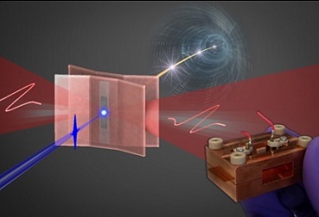
Ultrashort bursts of electrons have several important applications in scientific imaging, but producing them has typically required a costly, power-hungry apparatus about the size of a car.
In the journal Optica, researchers at MIT, the German Synchrotron, and the University of Hamburg in Germany describe a new technique for generating electron bursts, which could be the basis of a shoebox-sized device that consumes only a fraction as much power as its predecessors.
Ultrashort electron beams are used to directly gather information about materials that are undergoing chemical reactions or changes of physical state. But after being fired down a particle accelerator a half a mile long, they’re also used to produce ultrashort X-rays.
Last year, in Nature Communications, the same group of MIT and Hamburg researchers reported the prototype of a small “linear accelerator” that could serve the same purpose as the much larger and more expensive particle accelerator. That technology, together with a higher-energy version of the new “electron gun,” could bring the imaging power of ultrashort X-ray pulses to academic and industry labs.
Indeed, while the electron bursts reported in the new paper have a duration measured in hundreds of femtoseconds, or quadrillionths of a second (which is about what the best existing electron guns can manage), the researchers’ approach has the potential to lower their duration to a single femtosecond. An electron burst of a single femtosecond could generate attosecond X-ray pulses, which would enable real-time imaging of cellular machinery in action.
“We’re building a tool for the chemists, physicists, and biologists who use X-ray light sources or the electron beams directly to do their research,” says Ronny Huang, an MIT PhD student in electrical engineering and first author on the new paper. “Because these electron beams are so short, they allow you to kind of freeze the motion of electrons inside molecules as the molecules are undergoing a chemical reaction. A femtosecond X-ray light source requires more hardware, but it utilizes electron guns.”
In particular, Huang explains, with a technique called electron diffraction imaging, physicists and chemists use ultrashort bursts of electrons to investigate phase changes in materials, such as the transition from an electrically conductive to a nonconductive state, and the creation and dissolution of bonds between molecules in chemical reactions.
Ultrashort X-ray pulses have the same advantages that ordinary X-rays do: They penetrate more deeply into thicker materials. The current method for producing ultrashort X-rays involves sending electron bursts from a car-sized electron gun through a billion-dollar, kilometer-long particle accelerator that increases their velocity. Then they pass between two rows of magnets — known as an “undulator” — that converts them to X-rays.
In the paper published last year — on which Huang was a coauthor — the MIT-Hamburg group, together with colleagues from the Max Planck Institute for the Structure and Dynamics of Matter in Hamburg and the University of Toronto, described a new approach to accelerating electrons that could shrink particle accelerators to tabletop size. “This is supposed to complement that,” Huang says, about the new study.
Franz Kärtner, who was a professor of electrical engineering at MIT for 10 years before moving to the German Synchrotron and the University of Hamburg in 2011, led the project. Kärtner remains a principal investigator at MIT’s Research Laboratory of Electronics and is Huang’s thesis advisor. He and Huang are joined on the new paper by eight colleagues from both MIT and Hamburg.
Subwavelength confinement
The researchers’ new electron gun is a variation on a device called an RF gun. But where the RF gun uses radio frequency (RF) radiation to accelerate electrons, the new device uses terahertz radiation, the band of electromagnetic radiation between microwaves and visible light.
The researchers’ device, which is about the size of a matchbox, consists of two copper plates that, at their centers, are only 75 micrometers apart. Each plate has two bends in it, so that it looks rather like a trifold letter that’s been opened and set on its side. The plates bend in opposite directions, so that they’re farthest apart — 6 millimeters — at their edges.
At the center of one of the plates is a quartz slide on which is deposited a film of copper that, at its thinnest, is only 30 nanometers thick. A short burst of light from an ultraviolet laser strikes the film at its thinnest point, jarring loose electrons, which are emitted on the opposite side of the film.
At the same time, a burst of terahertz radiation passes between the plates in a direction perpendicular to that of the laser. All electromagnetic radiation can be thought of as having electrical and magnetic components, which are perpendicular to each other. The terahertz radiation is polarized so that its electric component accelerates the electrons directly toward the second plate.
The key to the system is that the tapering of the plates confines the terahertz radiation to an area — the 75-micrometer gap — that is narrower than its own wavelength. “That’s something special,” Huang says. “Typically, in optics, you can’t confine something to below a wavelength. But using this structure we were able to. Confining it increases the energy density, which increases the accelerating power.”
Because of that increased accelerating power, the device can make do with terahertz beams whose power is much lower than that of the radio-frequency beams used in a typical RF gun. Moreover, the same laser can generate both the ultraviolet beam and, with a few additional optical components, the terahertz beam.
According to James Rosenzweig, a professor of physics at the University of California at Los Angeles, that’s one of the most attractive aspects of the researchers’ system. “One of the main problems you have with ultrafast sources like this is timing jitter between, say, the laser and accelerating field, which produces all sorts of systematic effects that make it harder to do time-resolved electron diffraction,” Rosezweig says.
“In the case of Kärtner’s device, the laser produces the terahertz and also produces the photoelectrons, so the jitter is highly suppressed. You could do pump-probe experiments where the laser is the driver and the electrons would be the probe, and they would be more successful than what you have right now. And of course it would be a very small-sized and modest-cost device. So it might turn out to be very important as far as that scenario goes.”
The researchers’ work was funded by the U.S. Air Force Office of Scientific Research and by the European Research Council. Ronny Huang was supported by a National Defense Science and Engineering Graduate fellowship.
Share on:


Testimonial
"We’re proud to call I-Connect007 a trusted partner. Their innovative approach and industry insight made our podcast collaboration a success by connecting us with the right audience and delivering real results."
Julia McCaffrey - NCAB GroupSuggested Items
Trouble in Your Tank: Implementing Direct Metallization in Advanced Substrate Packaging
09/15/2025 | Michael Carano -- Column: Trouble in Your TankDirect metallization systems based on conductive graphite are gaining popularity throughout the world. The environmental and productivity gains achievable with this process are outstanding. Direct metallization reduces the costs of compliance, waste treatment, and legal issues related to chemical exposure. A graphite-based direct plate system has been devised to address these needs.
Closing the Loop on PCB Etching Waste
09/09/2025 | Shawn Stone, IECAs the PCB industry continues its push toward greener, more cost-efficient operations, Sigma Engineering’s Mecer System offers a comprehensive solution to two of the industry’s most persistent pain points: etchant consumption and rinse water waste. Designed as a modular, fully automated platform, the Mecer System regenerates spent copper etchants—both alkaline and acidic—and simultaneously recycles rinse water, transforming a traditionally linear chemical process into a closed-loop system.
Driving Innovation: Depth Routing Processes—Achieving Unparalleled Precision in Complex PCBs
09/08/2025 | Kurt Palmer -- Column: Driving InnovationIn PCB manufacturing, the demand for increasingly complex and miniaturized designs continually pushes the boundaries of traditional fabrication methods, including depth routing. Success in these applications demands not only on robust machinery but also sophisticated control functions. PCB manufacturers rely on advanced machine features and process methodologies to meet their precise depth routing goals. Here, I’ll explore some crucial functions that empower manufacturers to master complex depth routing challenges.
Trouble in Your Tank: Minimizing Small-via Defects for High-reliability PCBs
08/27/2025 | Michael Carano -- Column: Trouble in Your TankTo quote the comedian Stephen Wright, “If at first you don’t succeed, then skydiving is not for you.” That can be the battle cry when you find that only small-diameter vias are exhibiting voids. Why are small holes more prone to voids than larger vias when processed through electroless copper? There are several reasons.
The Government Circuit: Navigating New Trade Headwinds and New Partnerships
08/25/2025 | Chris Mitchell -- Column: The Government CircuitAs global trade winds continue to howl, the electronics manufacturing industry finds itself at a critical juncture. After months of warnings, the U.S. Government has implemented a broad array of tariff increases, with fresh duties hitting copper-based products, semiconductors, and imports from many nations. On the positive side, tentative trade agreements with Europe, China, Japan, and other nations are providing at least some clarity and counterbalance.