


 The Marketing Minute: Cracking the Code of Technical Marketing
 Trouble in Your Tank: Implementing Direct Metallization in Advanced Substrate Packaging


Designer Materials Create Miniature Computer Circuits
November 22, 2016 | University of ManchesterEstimated reading time: 1 minute
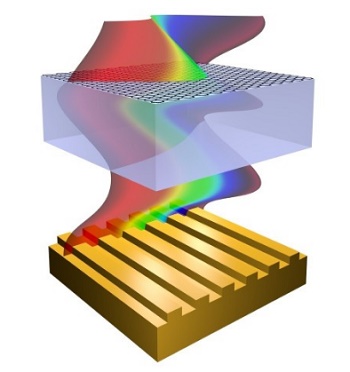
Scientists at The University of Manchester have discovered a new method of creating optoelectronic circuits using graphene and other 2D materials that are much smaller than their current counterparts.
Optoelectronics, the technology that uses pulses of light rather than traditional electrical signals, is vital for telecommunication networks.
Modulators are important in optoelectronic circuits as they control the signals passed through optoelectronic devices. Previous attempts to create hybrid modulators incorporating graphene have yielded promising although limited results.
Writing in Nature Communications, researchers led by Professor Sasha Grigorenko have shown it is possible to combine graphene, its sister material boron nitride and a nanoscale gold grating to create a new class of optical modulator.
Graphene is the world’s first two-dimensional material, just one atom thick yet 200 times stronger than steel, more conductive than copper and impermeable to water.
Since then a whole family of 2D materials have been uncovered and are now being used together in order to tailor materials to meet specific requirements.
The proposed device can effectively process information using light much the same way as computers process information using electrons.
Graphene NOWNANO PhD student Philip Thomas, who led the experimental work, said: “This could pave the way for faster circuits, which is the main selling point of using light instead of electrical signals. But probably the bigger result from this work is that it could allow for a dramatic reduction in the size of these circuits. It is rare to have a modulator which both creates a strong modulation effect and is really tiny.”
Professor Sasha Grigorenko said: “It is unprecedented to achieve light modulation in such a wide wavelength range - from visible to infrared light in which human eye, night vision goggles and thermal imaging operate - using just one simple design.”
Share on:


Testimonial
"We’re proud to call I-Connect007 a trusted partner. Their innovative approach and industry insight made our podcast collaboration a success by connecting us with the right audience and delivering real results."
Julia McCaffrey - NCAB GroupSuggested Items
Trouble in Your Tank: Implementing Direct Metallization in Advanced Substrate Packaging
09/15/2025 | Michael Carano -- Column: Trouble in Your TankDirect metallization systems based on conductive graphite are gaining popularity throughout the world. The environmental and productivity gains achievable with this process are outstanding. Direct metallization reduces the costs of compliance, waste treatment, and legal issues related to chemical exposure. A graphite-based direct plate system has been devised to address these needs.
Closing the Loop on PCB Etching Waste
09/09/2025 | Shawn Stone, IECAs the PCB industry continues its push toward greener, more cost-efficient operations, Sigma Engineering’s Mecer System offers a comprehensive solution to two of the industry’s most persistent pain points: etchant consumption and rinse water waste. Designed as a modular, fully automated platform, the Mecer System regenerates spent copper etchants—both alkaline and acidic—and simultaneously recycles rinse water, transforming a traditionally linear chemical process into a closed-loop system.
Driving Innovation: Depth Routing Processes—Achieving Unparalleled Precision in Complex PCBs
09/08/2025 | Kurt Palmer -- Column: Driving InnovationIn PCB manufacturing, the demand for increasingly complex and miniaturized designs continually pushes the boundaries of traditional fabrication methods, including depth routing. Success in these applications demands not only on robust machinery but also sophisticated control functions. PCB manufacturers rely on advanced machine features and process methodologies to meet their precise depth routing goals. Here, I’ll explore some crucial functions that empower manufacturers to master complex depth routing challenges.
Trouble in Your Tank: Minimizing Small-via Defects for High-reliability PCBs
08/27/2025 | Michael Carano -- Column: Trouble in Your TankTo quote the comedian Stephen Wright, “If at first you don’t succeed, then skydiving is not for you.” That can be the battle cry when you find that only small-diameter vias are exhibiting voids. Why are small holes more prone to voids than larger vias when processed through electroless copper? There are several reasons.
The Government Circuit: Navigating New Trade Headwinds and New Partnerships
08/25/2025 | Chris Mitchell -- Column: The Government CircuitAs global trade winds continue to howl, the electronics manufacturing industry finds itself at a critical juncture. After months of warnings, the U.S. Government has implemented a broad array of tariff increases, with fresh duties hitting copper-based products, semiconductors, and imports from many nations. On the positive side, tentative trade agreements with Europe, China, Japan, and other nations are providing at least some clarity and counterbalance.