


 The Marketing Minute: Cracking the Code of Technical Marketing
 Trouble in Your Tank: Implementing Direct Metallization in Advanced Substrate Packaging


New Ultra-Thin Semiconductor Could Extend Life of Moore’s Law
November 22, 2016 | University of ManchesterEstimated reading time: 2 minutes
Following a decade of intensive research into graphene and two-dimensional materials a new semiconductor material shows potential for the future of super-fast electronics.
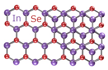
The new semiconductor named Indium Selenide (InSe) is only a few atoms thick, similarly to graphene. The research was reported in Nature Nanotechnology this week by researchers of The University of Manchester and their colleagues at The University of Nottingham.
Graphene is just one atom thick and has unrivalled electronic properties, which has led to widely-publicised suggestions about its use in future electronic circuits.
For all its superlative properties graphene has no energy gap. It behaves more like a metal rather than a normal semiconductor, frustrating its potential for transistor-type applications.
The new research shows that InSe crystals can be made only a few atoms thick, nearly as thin as graphene. InSe was shown to have electronic quality higher than that of silicon which is ubiquitously used in modern electronics.
Importantly, unlike graphene but similar to silicon, ultra-thin InSe has a large energy gap allowing transistors to be easily switched on and off, allowing for super-fast next-generation electronic devices.
Combining graphene with other new materials, which individually have excellent characteristics complementary to the extraordinary properties of graphene, has resulted in exciting scientific developments and could produce applications as yet beyond our imagination.
Sir Andre Geim, one of the authors of this study and a recipient of the Nobel Prize in Physics for research on graphene, believes that the new findings could have a significant impact on development of future electronics.
“Ultra-thin InSe seems to offer the golden middle between silicon and graphene. Similar to graphene, InSe offers a naturally thin body, allowing scaling to the true nanometre dimensions. Similar to silicon, InSe is a very good semiconductor.”
The Manchester researchers had to overcome one major problem to create high-quality InSe devices. Being so thin, InSe is rapidly damaged by oxygen and moisture present in the atmosphere. To avoid such damage, the devices were prepared in an argon atmosphere using new technologies developed at the National Graphene Institute.
This allowed high-quality atomically-thin films of InSe for the first time. The electron mobility at room temperature was measured at 2,000 cm2/Vs, significantly higher than silicon. This value increases several times at lower temperatures.
Current experiments produced the material several micrometres in size, comparable to the cross-section of a human hair. The researchers believe that by following the methods now widely used to produce large-area graphene sheets, InSe could also soon be produced at a commercial level.
Co-author of the paper Professor Vladimir Falko, Director of the National Graphene Institute said: “The technology that the NGI has developed for separating atomic layers of materials into high-quality two-dimensional crystals offers great opportunities to create new material systems for optoelectronics applications. We are constantly looking for new layered materials to try.”
Ultra-thin InSe is one of a growing family of two-dimensional crystals that have a variety of useful properties depending on their structure, thickness and chemical composition.
Currently, research in graphene and related two-dimensional materials is the fastest growing field of materials science that bridges science and engineering.
Share on:


Testimonial
"In a year when every marketing dollar mattered, I chose to keep I-Connect007 in our 2025 plan. Their commitment to high-quality, insightful content aligns with Koh Young’s values and helps readers navigate a changing industry. "
Brent Fischthal - Koh YoungSuggested Items
Curing and Verification in PCB Shadow Areas
09/17/2025 | Doug Katze, DymaxDesign engineers know a simple truth that often complicates electronics manufacturing: Light doesn’t go around corners. In densely populated PCBs, adhesives and coatings often fail to fully cure in shadowed regions created by tall ICs, connectors, relays, and tight housings.
Marcy’s Musings: Advancing the Advanced Materials Discussion
09/17/2025 | Marcy LaRont -- Column: Marcy's MusingsAs the industry’s most trusted global source of original content about the electronics supply chain, we continually ask you about your concerns, what you care about, and what you most want to learn about. Your responses are insightful and valuable. Thank you for caring enough to provide useful feedback and engage in dialogue.
September 2025 PCB007 Magazine: The Future of Advanced Materials
09/16/2025 | I-Connect007 Editorial TeamMoore’s Law is no more, and the advanced material solutions being developed to grapple with this reality are surprising, stunning, and perhaps a bit daunting. Buckle up for a dive into advanced materials and a glimpse into the next chapters of electronics manufacturing.
I-Connect007 Launches Advanced Electronics Packaging Digest
09/15/2025 | I-Connect007I-Connect007 is pleased to announce the launch of Advanced Electronics Packaging Digest (AEPD), a new monthly digital newsletter dedicated to one of the most critical and rapidly evolving areas of electronics manufacturing: advanced packaging at the interconnect level.
Panasonic Industry will Double the Production Capacity of MEGTRON Multi-layer Circuit Board Materials Over the Next Five Years
09/15/2025 | Panasonic Industry Co., Ltd.Panasonic Industry Co., Ltd., a Panasonic Group company, announced plans for a major expansion of its global production capacity for MEGTRON multi-layer circuit board materials today. The company plans to double its production over the next five years to meet growing demand in the AI server and ICT infrastructure markets.