


 The Marketing Minute: Cracking the Code of Technical Marketing
 Trouble in Your Tank: Implementing Direct Metallization in Advanced Substrate Packaging


New Solution for Making 2D Nanomaterials
November 22, 2016 | University of BristolEstimated reading time: 3 minutes
Two-dimensional (2D) nanomaterials have been made by dissolving layered materials in liquids, according to new UCL-led research which was supported by scientists from the University of Bristol.
The liquids can be used to apply the 2D nanomaterials over large areas and at low costs, enabling a variety of important future applications.
2D nanomaterials, such as graphene, have the potential to revolutionise technology through their remarkable physical properties, but their translation into real world applications has been limited due to the challenges of making and manipulating 2D nanomaterials on an industrial scale.
The new approach, published today in Nature Chemistry, produced single layers of many 2D nanomaterials in a scalable way. The researchers used the method on a wide variety of materials, including those with semiconductor and thermoelectric properties, to create 2D materials that could be used in solar cells or for turning wasted heat energy into electrical energy, for example.
Study Director, Dr Chris Howard (UCL Physics and Astronomy), said: "2D nanomaterials have outstanding properties and a unique size, which suggests they could be used in everything from computer displays to batteries to smart textiles.
"Many methods for making and applying 2D nanomaterials are difficult to scale or can damage the material, but we’ve successfully addressed some of these issues. Hopefully our new process will help us realise the potential of 2D nanomaterials in the future."
For the study, funded by the Royal Academy of Engineering and the Engineering and Physical Sciences Research Council, the scientists inserted positively charged lithium and potassium ions between the layers of different materials including bismuth telluride (Bi2Te3), molybdenum disulphide (MoS2) and titanium disulphide (TiS2), giving each layer a negative charge and creating a ‘'ayered material salt'.
These layered material salts were then gently dissolved in selected solvents without using chemical reactions or stirring. This gave solutions of 2D nanomaterial sheets with the same shape as the starting material but with a negative charge.
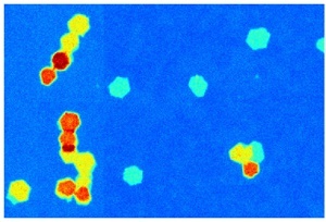
The scientists analysed the contents of the solutions using atomic force microscopy and transmission electron microscopy to investigate the structure and thickness of the 2D nanomaterials. They found that the layered materials dissolved into tiny sheets of clean, undamaged, single layers, isolated in solutions.
The team from UCL, University of Bristol, Cambridge Graphene Centre and École Polytechnique Fédérale de Lausanne, were able to demonstrate that even the 2D nanomaterial sheets, comprising millions of atoms, made stable solutions rather than suspensions.
Ground breaking analysis of these 2D materials was carried out by Dr Oliver Payton and Dr Loren Picco jointly between the Merchant Venturers’ School of Engineering and the Interface Analysis Centre at the University of Bristol’s School of Physics.
Using a high-speed atomic force microscope they were able to measure the distribution of layer thickness and 2D flake areas with unprecedented statistical confidence and speed.
These measurements were critical for the optimisation of the new production process and could provide an excellent route towards large scale quality assurance, necessary for upscaling the production of these exciting new materials.
Dr Oliver Payton said: "Our instrument is the fastest 3d super-resolution microscope in the world and enabled us to measure tens of thousands of these nanoscale 2d flakes at a time - something that conventional scanning probe microscopes are simply too slow to achieve.
"Our measurements are significantly more accurate than competing techniques and have helped the team to perfect this exciting new manufacturing process."
First author, Dr Patrick Cullen (UCL Chemical Engineering) said: "We didn't expect such a range of 2D nanomaterials to form a solution when we simply added the solvent to the salt – the layered material salts are large but dissolve into liquid similar to table salt in water. The fact that they form a liquid along with their negative charge, makes them easy to manipulate and use on a large scale, which is scientifically intriguing but also relevant to many industries.
"We've shown they can be painted onto surfaces and, when left to dry, can arrange themselves into different tiled shapes, which hasn't been seen before. They can also be electroplated onto surfaces in much the same way gold is used to plate metals. We’re looking forward to making different 2D nanomaterials using our process and trying them out in different applications as the possibilities are near endless."
UCL Business PLC (UCLB), the technology commercialisation company of UCL has patented this research and will be supporting the commercialisation process.
Share on:


Testimonial
"In a year when every marketing dollar mattered, I chose to keep I-Connect007 in our 2025 plan. Their commitment to high-quality, insightful content aligns with Koh Young’s values and helps readers navigate a changing industry. "
Brent Fischthal - Koh YoungSuggested Items
Curing and Verification in PCB Shadow Areas
09/17/2025 | Doug Katze, DymaxDesign engineers know a simple truth that often complicates electronics manufacturing: Light doesn’t go around corners. In densely populated PCBs, adhesives and coatings often fail to fully cure in shadowed regions created by tall ICs, connectors, relays, and tight housings.
Marcy’s Musings: Advancing the Advanced Materials Discussion
09/17/2025 | Marcy LaRont -- Column: Marcy's MusingsAs the industry’s most trusted global source of original content about the electronics supply chain, we continually ask you about your concerns, what you care about, and what you most want to learn about. Your responses are insightful and valuable. Thank you for caring enough to provide useful feedback and engage in dialogue.
September 2025 PCB007 Magazine: The Future of Advanced Materials
09/16/2025 | I-Connect007 Editorial TeamMoore’s Law is no more, and the advanced material solutions being developed to grapple with this reality are surprising, stunning, and perhaps a bit daunting. Buckle up for a dive into advanced materials and a glimpse into the next chapters of electronics manufacturing.
I-Connect007 Launches Advanced Electronics Packaging Digest
09/15/2025 | I-Connect007I-Connect007 is pleased to announce the launch of Advanced Electronics Packaging Digest (AEPD), a new monthly digital newsletter dedicated to one of the most critical and rapidly evolving areas of electronics manufacturing: advanced packaging at the interconnect level.
Panasonic Industry will Double the Production Capacity of MEGTRON Multi-layer Circuit Board Materials Over the Next Five Years
09/15/2025 | Panasonic Industry Co., Ltd.Panasonic Industry Co., Ltd., a Panasonic Group company, announced plans for a major expansion of its global production capacity for MEGTRON multi-layer circuit board materials today. The company plans to double its production over the next five years to meet growing demand in the AI server and ICT infrastructure markets.