


 The Marketing Minute: AI Is Watching Your Marketing Habits
 Trouble in Your Tank: The Role of Organic Solderability Preservatives in Advanced Packaging
 It’s Only Common Sense: Lighten Up!


It may be unwise to judge a book by its cover, but you can tell a lot about a material from the outermost electrons in its atoms.
“These outermost electrons, known as valence electrons, are the most important players in forming chemical bonds and actually define almost every property of a solid – electrical, thermal, conductive,” said Shambhu Ghimire, an associate staff scientist at the Department of Energy’s SLAC National Accelerator Laboratory.
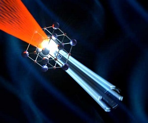
In experiments at SLAC, intense laser light (red) shining through a magnesium oxide crystal excited the outermost “valence” electrons of oxygen atoms deep inside it. When these electrons hit neighboring atoms, the collisions generated light of much higher energy and shorter wavelengths (blue) through a process called high harmonic generation. Rotating the crystal and analyzing the generated light revealed the density of the neighboring atom’s valence electrons, which could not be directly seen before. (Image: SLAC National Accelerator Laboratory)
Now Ghimire and two colleagues at the Stanford PULSE Institute have invented a new way to probe the valence electrons of atoms deep inside a crystalline solid.
In a report in Nature Physics ("Anisotropic high-harmonic generation in bulk crystals"), they describe using laser light to excite some of the valence electrons, steer them around inside the crystal and bounce them off other atoms. This produces high-energy bursts of light that are invisible to our eyes, but carry clues to the material’s atomic structure and function.
“This will change the world of imaging the inside of crystalline solids,” Ghimire said, “much as scanning tunneling microscopy, or STM, changed the atomic-scale imaging of surfaces.”
intense laser light (red) shining through a magnesium oxide crystal excited the outermost valence electrons of oxygen atoms deep inside it
A New Way to Look at Atoms in Solids
Invented in the early 1980s, STM was a revolutionary method that allowed scientists to make the first images of individual atoms and their bonds. It was honored with the 1986 Nobel Prize in physics.
But STM senses valence electrons from only the top two or three layers of atoms in a material. A flow of those electrons into the instrument’s tip creates a current that allows it to measure the distance between the tip and the surface, tracing the bumps where atoms poke up and the valleys between them. This creates an image of the atoms and yields information about the bonds that hold them together.
Now the new technique will give scientists the same level of access to the valence electrons deep inside the solid.
The experiments, carried out in a SLAC laser lab by PULSE postdoctoral researcher Yong Sing You, involved crystals of magnesium oxide or magnesia, a common mineral used to make cement, preserve library books and clean up contaminated soil, among a host of other things.
These crystals also have the ability to shift incoming laser light to much shorter wavelengths and higher energies – much as pressing down on a guitar string produces a higher note – through a process called high harmonic generation, or HHG.
Steering Electrons to Generate Light
In this case, the scientists carefully adjusted the incoming infrared laser beam so it would excite valence electrons in the crystal’s oxygen atoms. Those electrons oscillated, like vibrating guitar strings, and generated light of much shorter wavelengths – in the extreme ultraviolet range – through HHG.
But when they adjusted the polarization of the laser beam to steer the excited electrons along different trajectories within the crystal, they discovered that HHG only took place when an electron hit a neighboring atom, and was most efficient when it hit the atom dead center. Further, the wavelength of the harmonically generated light coming out – which was 13 to 21 times shorter than the light that went in – revealed the density of the neighboring atom’s valence electrons, the size of the atom and even whether it was an atom of oxygen or magnesium.
“It’s difficult to home in on the valence electrons with current methods of measuring electron charge density, which typically use X-ray or electron diffraction,” said study co-author David Reis, an associate professor at SLAC and Stanford and deputy director of PULSE. “So demonstrating that we can do that with atomic-scale sensitivity in a tabletop laser experiment is an important milestone.”
Alan Fry, division director for laser science and technology at SLAC’s Linac Coherent Light Source X-ray laser, was not involved in the experiment but offered kudos “to the team that developed this technique and who continue to do exciting and interesting research with it.”
While this approach may be limited to materials that can generate light through HHG, he said, “it can still tell you a lot about the electronic structure inside those solids, and in principle could give us a better understanding of other materials that don't have same response. Understanding simple systems like this builds a foundation for understanding more complex systems.”


