


 Dan's Biz Bookshelf: 'Getting Naked: A Business Fable'
 The Chemical Connection: Common Misconceptions in Wet Processing
 It’s Only Common Sense: Selling to Engineers


Squeezing Light Into New Miniature Devices
November 28, 2016 | Institute for Basic ScienceEstimated reading time: 2 minutes
Do you think your computer is fast enough? Think again. The computers of the future could work almost at the speed of light! Nanophotonics, the study of light at the nanometer scale, could indeed bring the speed of our technology to a completely different level.
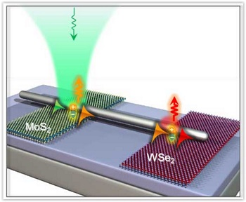
The multiplexer device with one input and two outputs. The plus-minus couple indicates the exciton.
The Center for Integrated Nanostructure Physics (CINAP) within the Institute for Basic Science (IBS) have developed three key components of a circuit that works with light. Published in Nature Communications ("Reconfigurable exciton-plasmon interconversion for nanophotonic circuits"), these devices combine the advantages of photonics and electronics on the same platform.
While we are slowing approaching the end point of Moore's Law: a state where we physically cannot shrink the dimension of our transistors much further; the future of big data processing requires high performance computers with higher speed operations. Researchers reckon that if we build computers that process information through light, instead of electrons, computer will be able to work faster.
However, at nanometer dimensions, the wavelength of light is larger than the diameter of the silicon fiber and for this reason some light can be lost. A solution to control the propagation of light in matter can come from surface plasmons. These are electromagnetic waves that propagate along the surface of some conductive materials like silver, gold, aluminum and copper. Using surface plasmons, optical information can be transmitted nearly at the speed of light and in extremely miniature volumes.
Using surface plasmons in silver nanowires and 2D semiconductors like molybdenum disulphide (MoS2), IBS scientists built three key components for optical communication: optical transistors, optical multiplexers and optical signal detectors.
These devices work thanks to a phenomenon called plasmon-exciton-plasmon interconversion. The graphics describe the details of this process step-by-step.
IBS scientists constructed the optical transistor by interconnecting the silver nanowire to a flake of MoS2. Light shone on the device is converted to surface plasmon, than to exciton, back to surface plasmon and eventually emitted as light with a shorter wavelength compared to the initial input. For example, if the input light is green, the output light can be red.
Wavelength multiplexing devices were realized in a similar way, but instead of having only a flake of MoS2, the researchers used an array of three different 2D semiconductor materials emitting light at different wavelengths. In this structure, for example, a single input light (violet color) generates three output lights (blue, green and red).
The propagating optical signals along the silver nanowire can be also transformed and detected as electrical signals by an optical signal detector.
“The originality of this paper arises from the exciton-plasmon interconversion. We published before the conversion of exciton to plasmon, and from plasmon to exciton using silver nanowire/2D semiconductor hybrids, but this is the first time that we can complete the circle going from plasmons to excitons and back to plasmons. Using this concept, we created optical transistors and multiplexors,” explains professor Hyun Seok Lee, first author of this study.
Share on:


Suggested Items
Elephantech: For a Greener Tomorrow
04/16/2025 | Marcy LaRont, PCB007 MagazineNobuhiko Okamoto is the global sales and marketing manager for Elephantech Inc., a Japanese startup with a vision to make electronics more sustainable. The company is developing a metal inkjet technology that can print directly on the substrate and then give it a copper thickness by plating. In this interview, he discusses this novel technology's environmental advantages, as well as its potential benefits for the PCB manufacturing and semiconductor packaging segments.
Trouble in Your Tank: Organic Addition Agents in Electrolytic Copper Plating
04/15/2025 | Michael Carano -- Column: Trouble in Your TankThere are numerous factors at play in the science of electroplating or, as most often called, electrolytic plating. One critical element is the use of organic addition agents and their role in copper plating. The function and use of these chemical compounds will be explored in more detail.
IDTechEx Highlights Recyclable Materials for PCBs
04/10/2025 | IDTechExConventional printed circuit board (PCB) manufacturing is wasteful, harmful to the environment and energy intensive. This can be mitigated by the implementation of new recyclable materials and technologies, which have the potential to revolutionize electronics manufacturing.
Connect the Dots: Stop Killing Your Yield—The Hidden Cost of Design Oversights
04/03/2025 | Matt Stevenson -- Column: Connect the DotsI’ve been in this industry long enough to recognize red flags in PCB designs. When designers send over PCBs that look great on the computer screen but have hidden flaws, it can lead to manufacturing problems. I have seen this happen too often: manufacturing delays, yield losses, and designers asking, “Why didn’t anyone tell me sooner?” Here’s the thing: Minor design improvements can greatly impact manufacturing yield, and design oversights can lead to expensive bottlenecks. Here’s how to find the hidden flaws in a design and avoid disaster.
Real Time with... IPC APEX EXPO 2025: Tariffs and Supply Chains in U.S. Electronics Manufacturing
04/01/2025 | Real Time with...IPC APEX EXPOChris Mitchell, VP of Global Government Relations for IPC, discusses IPC's concerns about tariffs on copper and their impact on U.S. electronics manufacturing. He emphasizes the complexity of supply chains and the need for policymakers to understand their effects.