


 The Marketing Minute: Cracking the Code of Technical Marketing
 Trouble in Your Tank: Implementing Direct Metallization in Advanced Substrate Packaging


Metamaterials Open up Entirely New Possibilities in Optics
November 29, 2016 | CHALMERS UNIVERSITY OF TECHNOLOGYEstimated reading time: 1 minute
Researchers at Chalmers University of Technology have developed a method that enables them to manipulate light to follow any predetermined path along a surface. The innovation has now been described as one of the world’s 30 most exciting discoveries within optics and photonics during 2016.
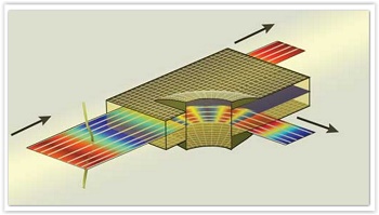
Illustration of a light bender based on the newly proposed technique: light propagates along the surface of an optical chip and flows into a metamaterial layer from the left. Thanks to a specific thickness variation, the light is either bent to the right or allowed to propagate straight through towards the exit of the optical chip without being disrupted. (Illustration: Sophie Viaene)
Earlier this year, Chalmers researchers Philippe Tassin and Sophie Viaene published their discovery about how light can be controlled with metamaterials. Amidst strong international competition, their paper has now been chosen as one of the best this year by the influential magazine, Optics & Photonics News ("Transforming two-dimensional guided light using nonmagnetic metamaterial waveguides").
The innovation from Chalmers University of Technology makes it possible to manipulate light to follow any predetermined path along a surface. With the help of a mathematical design tool it is possible to create various artificial materials – metamaterials – that guide the light along the path of your choice.
“We don’t have to think about the limitations of natural materials. Instead, we decide what we want to do and then we design a metamaterial waveguide that makes it work. This is beautiful physics, building on Einstein’s general theory of relativity,” says Sophie Viaene, PhD student in the Division of Condensed Matter Physics.
The new technique has a wide field of application. For example, it can be used in optical chips to achieve reliable data delivery on the internet, or to speed up routers.
“Our method opens up the toolbox of transformation optics to a plethora of waveguide-based devices,” says Philippe Tassin, Professor in the Division of Condensed Matter Physics.
In the future, the researchers hope that they can even improve how light is produced.
“For example, an LED lamp is far from perfect when it comes to energy efficiency. Metamaterials could extract light in a more efficient way – and maybe we can also manipulate the colour of light,” says Tassin.
Share on:


Testimonial
"In a year when every marketing dollar mattered, I chose to keep I-Connect007 in our 2025 plan. Their commitment to high-quality, insightful content aligns with Koh Young’s values and helps readers navigate a changing industry. "
Brent Fischthal - Koh YoungSuggested Items
Driving Innovation: Depth Routing Processes—Achieving Unparalleled Precision in Complex PCBs
09/08/2025 | Kurt Palmer -- Column: Driving InnovationIn PCB manufacturing, the demand for increasingly complex and miniaturized designs continually pushes the boundaries of traditional fabrication methods, including depth routing. Success in these applications demands not only on robust machinery but also sophisticated control functions. PCB manufacturers rely on advanced machine features and process methodologies to meet their precise depth routing goals. Here, I’ll explore some crucial functions that empower manufacturers to master complex depth routing challenges.
Polar Instruments Announces Additive Transmission Line Support for Si9000e
08/20/2025 | Polar InstrumentsTransmission lines embedded into the PCB surface are a feature of UHDI constructions. The 2025 fall release of Polar's Si9000e PCB impedance & insertion loss transmission line field solver incorporates eight new single ended, differential and coplanar transmission line structures.
Henniker Plasma Launches Stratus Turnkey Plasma Manufacturing Cell
08/13/2025 | Henniker PlasmaHenniker Plasma, a leading manufacturer of plasma treatment systems, proudly announces the launch of its Stratus Plasma Manufacturing Cell range — a fully integrated, turnkey solution that combines advanced atmospheric plasma surface treatment with robotic automation.
Trouble in Your Tank: Metallizing Flexible Circuit Materials—Mitigating Deposit Stress
08/04/2025 | Michael Carano -- Column: Trouble in Your TankMetallizing materials, such as polyimide used for flexible circuitry and high-reliability multilayer printed wiring boards, provide a significant challenge for process engineers. Conventional electroless copper systems often require pre-treatments with hazardous chemicals or have a small process window to achieve uniform coverage without blistering. It all boils down to enhancing the adhesion of the thin film of electroless copper to these smooth surfaces.
Designers Notebook: Basic PCB Planning Criteria—Establishing Design Constraints
07/22/2025 | Vern Solberg -- Column: Designer's NotebookPrinted circuit board development flows more smoothly when all critical issues are predefined and understood from the start. As a basic planning strategy, the designer must first consider the product performance criteria, then determine the specific industry standards or specifications that the product must meet. Planning also includes a review of all significant issues that may affect the product’s manufacture, performance, reliability, overall quality, and safety.