


 American Made Advocacy: Rebuilding America’s Military Stockpiles Begins With Microelectronics
 The Right Approach: The End of an Era—DoD Proposes MIL-PRF-31032 Cancellation
 Defense Speak Interpreted: Hypersonics Report Back After Six Years of Silence


Making Flawless Graphene Coatings
November 29, 2016 | University of LeidenEstimated reading time: 3 minutes
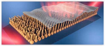
Graphene, the ultra-thin material just a single carbon atom in thickness, holds the promise of such impressive applications as wear-resistant, friction-free coatings. But first manufacturers have to be able to produce large sheets of graphene under precisely controlled conditions. Dirk van Baarle studied how graphene grows at atomic scale and what determines the friction with other materials. PhD defence 29 November.
Predictable quality
An almost perfectly friction-free, wear-resistant coating in machinery could generate enormous savings in fuel and maintenance. In the world of nano-technology such coatings will probably even have applications that we are currently not able to predict. In his PhD research Dirk van Baarle studied a candidate for such coatings: graphene. Van Baarle: 'It's quite a challenge to produce graphene of a predictable quality.'
Graphene is only super strong if the wire mesh of carbon atoms that make up the material are perfectly regular in form. But with the present production methods, a sheet of graphene is in practice almost always made up of a patchwork of small pieces that have been grafted onto one another. Van Baarle was able to observe almost per carbon atom live how islands of graphene grow towards one another and how this process is influenced by temperature and substrate. This is the first step towards a production method for making larger, flawless sheets of graphene.
Chicken wire pattern
Graphene occurs spontaneously when a very clean surface of iridium comes into contact with ethylene (C2H4, a hydrocarbon) at a temperature of around 700 degrees Celsius. The gas molecules disintegrate on the hot surface, leaving behind the carbon atoms, which spontaneously form a network of linked hexagons, in a chicken wire pattern.
For his research Van Baarle used a unique piece of equipment in the Huygens-Kamerlingh Onnes Laboratory, the VT-STM (Variable Temperature Scanning Tunneling Microscope). This apparatus comprises a minuscule stylus with a point that is just a few atoms thick. It can be used to systematically scan a surface with such a high degree of precision (what you are in fact doing is measuring the flow of electricity between the stylus and the surface) that even individual atoms can be distinguished. What makes the Leiden instrument unique is that it can do this even at high and variable temperatures.
A remarkable finding is that atomic processes occur not only in the growing layer of graphene. In practice, the surface of the iridium does not match the atomic layers in the substrate perfectly. The iridium forms broad steps on the surface, where the graphene grows over it. But these steps can continue to grow underneath the graphene or can withdraw as a result of the iridium atoms in the substrate realigning themselves. This process, too, has to be closely controlled in order to allow perfect sheets of graphene to form.
Contact points
In the theoretical part of his research, Van Baarle developed a model of how friction occurs at atomic level. When two surfaces slide over one another, the actual contact points are only nanometres in size, just a very few atoms. The friction is at its maximum when the stiffness of the nano-protrusions is roughly average: not too soft, but also not too stiff.
Van Baarle: 'One of my colleagues is currently coating an object with nano-needles using a lithography technique (a technique that is also used for computer chips). These needles vary in stiffness, depending on the direction in which they bend. This means that the friction of the surface is different in different directions.' This can be useful, for example, for a coating on a revolving axis, to prevent it moving laterally.
'Internally we are already using graphene coatings in our equipment to reduce friction without using lubricants,' Van Baarle explains. 'It has already resulted in a patent and a start-up, Applied Nanolayers. No wonder our professor, Joost Frenken, has already won a valorisation prize.'
Share on:


Testimonial
"Advertising in PCB007 Magazine has been a great way to showcase our bare board testers to the right audience. The I-Connect007 team makes the process smooth and professional. We’re proud to be featured in such a trusted publication."
Klaus Koziol - atgSuggested Items
Connect the Dots: Designing for the Future of Manufacturing Reality—Surface Finish
05/07/2026 | Matt Stevenson -- Column: Connect the DotsWhen designing the complex boards that many electronic devices require to operate, designers should consider manufacturability at every step. This is my last article focused on designing for the always-evolving manufacturing reality. Choosing the right surface finish has always been important. If you are creating intricate designs with a wide variety of components, like for an ultra-high density interconnect (UHDI) board, surface finish is a critical last step.
Elsyca Acquires Hivelix to Strengthen Simulation Platform for Electrochemical Surface Engineering
04/03/2026 | ElsycaElsyca, a global pioneer in computer-aided engineering (CAE) simulation for electrochemical processes and surface finishing, announces the acquisition of Hivelix, a specialist in advanced surface treatment simulation with strong expertise in multiphysics modelling and AI-assisted process optimisation.
Connect the Dots: Designing for the Future of Manufacturing Reality—Solder Mask and Legend
04/09/2026 | Matt Stevenson -- Column: Connect the DotsPCBs seem to be getting more complex by the day, so it is important for designers to keep educating themselves about the realities of manufacturing increasingly intricate boards. Last month’s column highlighted design considerations for the strip-etch-strip process and how manufacturers approach that phase of production. Now that we have a functioning board, we must protect the PCB from environmental hazards and document the circuit components. This article will detail the solder mask and legend process and offer best practices for designers to ensure a high-quality result.
Take the Mic: Photo Chemical Systems: 50 Years Strong
04/03/2026 | Real Time with... APEX EXPOPhoto Chemical Systems is celebrating 50 years in the bare board PCB market. David Graves and Jason Averette discuss how they've expanded into assembly, leveraging strong relationships and a customer-centric approach to navigate supply chain challenges. With innovative solutions and future growth strategies, including AI integration and new market ventures, Photo Chemical Systems continues enduring success.
Bold Laser Automation Introduces Precision Laser Cleaning System for Advanced Manufacturing
03/27/2026 | PRNewswireBold Laser Automation, Inc. has introduced the LPCl1820UV Laser Precision Cleaning System, a Class 1, industrial laser platform engineered for high-precision surface cleaning and thin-film removal in demanding manufacturing environments.