


 It’s Only Common Sense: 20 Lessons in 20 Years—A Career in Common Sense
 The Marketing Minute: Staying Positive When the Market Isn’t
 Marcy’s Musings: Continuing to Invent the Future With SEL


Making Flawless Graphene Coatings
November 29, 2016 | University of LeidenEstimated reading time: 3 minutes
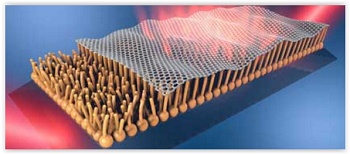
Graphene, the ultra-thin material just a single carbon atom in thickness, holds the promise of such impressive applications as wear-resistant, friction-free coatings. But first manufacturers have to be able to produce large sheets of graphene under precisely controlled conditions. Dirk van Baarle studied how graphene grows at atomic scale and what determines the friction with other materials. PhD defence 29 November.
Predictable quality
An almost perfectly friction-free, wear-resistant coating in machinery could generate enormous savings in fuel and maintenance. In the world of nano-technology such coatings will probably even have applications that we are currently not able to predict. In his PhD research Dirk van Baarle studied a candidate for such coatings: graphene. Van Baarle: 'It's quite a challenge to produce graphene of a predictable quality.'
Graphene is only super strong if the wire mesh of carbon atoms that make up the material are perfectly regular in form. But with the present production methods, a sheet of graphene is in practice almost always made up of a patchwork of small pieces that have been grafted onto one another. Van Baarle was able to observe almost per carbon atom live how islands of graphene grow towards one another and how this process is influenced by temperature and substrate. This is the first step towards a production method for making larger, flawless sheets of graphene.
Chicken wire pattern
Graphene occurs spontaneously when a very clean surface of iridium comes into contact with ethylene (C2H4, a hydrocarbon) at a temperature of around 700 degrees Celsius. The gas molecules disintegrate on the hot surface, leaving behind the carbon atoms, which spontaneously form a network of linked hexagons, in a chicken wire pattern.
For his research Van Baarle used a unique piece of equipment in the Huygens-Kamerlingh Onnes Laboratory, the VT-STM (Variable Temperature Scanning Tunneling Microscope). This apparatus comprises a minuscule stylus with a point that is just a few atoms thick. It can be used to systematically scan a surface with such a high degree of precision (what you are in fact doing is measuring the flow of electricity between the stylus and the surface) that even individual atoms can be distinguished. What makes the Leiden instrument unique is that it can do this even at high and variable temperatures.
A remarkable finding is that atomic processes occur not only in the growing layer of graphene. In practice, the surface of the iridium does not match the atomic layers in the substrate perfectly. The iridium forms broad steps on the surface, where the graphene grows over it. But these steps can continue to grow underneath the graphene or can withdraw as a result of the iridium atoms in the substrate realigning themselves. This process, too, has to be closely controlled in order to allow perfect sheets of graphene to form.
Contact points
In the theoretical part of his research, Van Baarle developed a model of how friction occurs at atomic level. When two surfaces slide over one another, the actual contact points are only nanometres in size, just a very few atoms. The friction is at its maximum when the stiffness of the nano-protrusions is roughly average: not too soft, but also not too stiff.
Van Baarle: 'One of my colleagues is currently coating an object with nano-needles using a lithography technique (a technique that is also used for computer chips). These needles vary in stiffness, depending on the direction in which they bend. This means that the friction of the surface is different in different directions.' This can be useful, for example, for a coating on a revolving axis, to prevent it moving laterally.
'Internally we are already using graphene coatings in our equipment to reduce friction without using lubricants,' Van Baarle explains. 'It has already resulted in a patent and a start-up, Applied Nanolayers. No wonder our professor, Joost Frenken, has already won a valorisation prize.'
Share on:


Testimonial
"Our marketing partnership with I-Connect007 is already delivering. Just a day after our press release went live, we received a direct inquiry about our updated products!"
Rachael Temple - AlltematedSuggested Items
Polar Instruments Announces Additive Transmission Line Support for Si9000e
08/20/2025 | Polar InstrumentsTransmission lines embedded into the PCB surface are a feature of UHDI constructions. The 2025 fall release of Polar's Si9000e PCB impedance & insertion loss transmission line field solver incorporates eight new single ended, differential and coplanar transmission line structures.
Henniker Plasma Launches Stratus Turnkey Plasma Manufacturing Cell
08/13/2025 | Henniker PlasmaHenniker Plasma, a leading manufacturer of plasma treatment systems, proudly announces the launch of its Stratus Plasma Manufacturing Cell range — a fully integrated, turnkey solution that combines advanced atmospheric plasma surface treatment with robotic automation.
Trouble in Your Tank: Metallizing Flexible Circuit Materials—Mitigating Deposit Stress
08/04/2025 | Michael Carano -- Column: Trouble in Your TankMetallizing materials, such as polyimide used for flexible circuitry and high-reliability multilayer printed wiring boards, provide a significant challenge for process engineers. Conventional electroless copper systems often require pre-treatments with hazardous chemicals or have a small process window to achieve uniform coverage without blistering. It all boils down to enhancing the adhesion of the thin film of electroless copper to these smooth surfaces.
Designers Notebook: Basic PCB Planning Criteria—Establishing Design Constraints
07/22/2025 | Vern Solberg -- Column: Designer's NotebookPrinted circuit board development flows more smoothly when all critical issues are predefined and understood from the start. As a basic planning strategy, the designer must first consider the product performance criteria, then determine the specific industry standards or specifications that the product must meet. Planning also includes a review of all significant issues that may affect the product’s manufacture, performance, reliability, overall quality, and safety.
Knocking Down the Bone Pile: Addressing End-of-life Component Solderability Issues, Part 4
07/16/2025 | Nash Bell -- Column: Knocking Down the Bone PileIn 1983, the Department of Defense identified that over 40% of military electronic system failures in the field were electrical, with approximately 50% attributed to poor solder connections. Investigations revealed that plated finishes, typically nickel or tin, were porous and non-intermetallic.