


 The Marketing Minute: Cracking the Code of Technical Marketing
 Trouble in Your Tank: Implementing Direct Metallization in Advanced Substrate Packaging


Researchers Explore New 2D Materials That Could Make Devices Faster, Smaller, and Efficient
November 29, 2016 | University of Minnesota College of Science and EngineeringEstimated reading time: 2 minutes
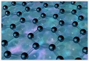
A new study by an international team of researchers led by the University of Minnesota highlights how manipulation of 2D materials could make our modern day devices faster, smaller, and better.
Two-dimensional materials are a class of nanomaterials that are only a few atoms in thickness. Electrons in these materials are free to move in the two-dimensional plane, but their restricted motion in the third direction is governed by quantum mechanics. Research on these nanomaterials is still in its infancy, but 2D materials such as graphene, transition metal dichalcogenides and black phosphorus have garnered tremendous attention from scientists and engineers for their amazing properties and potential to improve electronic and photonic devices.
In this study, researchers from the University of Minnesota, MIT, Stanford, U.S. Naval Research Laboratory, IBM, and universities in Brazil, UK and Spain, teamed up to examine the optical properties of several dozens of 2D materials. The goal of the paper is to unify understanding of light-matter interactions in these materials among researchers and explore new possibilities for future research.
They discuss how polaritons, a class of quasiparticles formed through the coupling of photons with electric charge dipoles in solid, allow researchers to marry the speed of photon light particles and the small size of electrons.
“With our devices, we want speed, efficiency, and we want small. Polaritons could offer the answer,” said Tony Low, a University of Minnesota electrical and computer engineering assistant professor and lead author of the study.
By exciting the polaritons in 2D materials, electromagnetic energy can be focused down to a volume a million times smaller compared to when its propagating in free space.
“Layered two-dimensional materials have emerged as a fantastic toolbox for nano-photonics and nano-optoelectronics, providing tailored design and tunability for properties that are not possible to realize with conventional materials,” said Frank Koppens, group leader at the Institute of Photonic Sciences at Barcelona, Spain, and co-author of the study. “This will offer tremendous opportunities for applications.”
Others on the team from private industry also recognize the potential in practical applications.
“The study of the plasmon-polaritons in two-dimensions is not only a fascinating research subject, but also offers possibilities for important technological applications,” said Phaedon Avoruris, IBM Fellow at the IBM T. J. Watson Research Center and co-author of the study. “For example, an atomic layer material like graphene extends the field of plasmonics to the infrared and terahertz regions of the electromagnetic spectrum allowing unique applications ranging from sensing and fingerprinting minute amounts of biomolecules, to applications in optical communications, energy harvesting and security imaging.”
The new study also examined the possibilities of combining 2D materials. Researchers point out that every 2D material has advantages and disadvantages. Combining these materials create new materials that may have the best qualities of both.
“Every time we look at a new material, we find something new,” Low said. “Graphene is often considered a ‘wonder’ material, but combining it with another material may make it even better for a wide variety of applications.”
In addition to Low, Avoruris and Koppens, other researchers involved in the study include Andrey Chaves, Universidade Federal do Cearán (Brazil) and Columbia University; Joshua D. Caldwell, U.S. Naval Research Laboratory; Anshuman Kumar, University of Minnesota and Massachusetts Institute of Technology; Nicholas X.Fang, MIT; Tony Heinz, Stanford University; Francisco Guinea, IMDEA Nanociencia and University of Manchester; and Luis Martin-Moreno, University of Zaragoza (Spain).
Share on:


Testimonial
"In a year when every marketing dollar mattered, I chose to keep I-Connect007 in our 2025 plan. Their commitment to high-quality, insightful content aligns with Koh Young’s values and helps readers navigate a changing industry. "
Brent Fischthal - Koh YoungSuggested Items
Curing and Verification in PCB Shadow Areas
09/17/2025 | Doug Katze, DymaxDesign engineers know a simple truth that often complicates electronics manufacturing: Light doesn’t go around corners. In densely populated PCBs, adhesives and coatings often fail to fully cure in shadowed regions created by tall ICs, connectors, relays, and tight housings.
Marcy’s Musings: Advancing the Advanced Materials Discussion
09/17/2025 | Marcy LaRont -- Column: Marcy's MusingsAs the industry’s most trusted global source of original content about the electronics supply chain, we continually ask you about your concerns, what you care about, and what you most want to learn about. Your responses are insightful and valuable. Thank you for caring enough to provide useful feedback and engage in dialogue.
September 2025 PCB007 Magazine: The Future of Advanced Materials
09/16/2025 | I-Connect007 Editorial TeamMoore’s Law is no more, and the advanced material solutions being developed to grapple with this reality are surprising, stunning, and perhaps a bit daunting. Buckle up for a dive into advanced materials and a glimpse into the next chapters of electronics manufacturing.
I-Connect007 Launches Advanced Electronics Packaging Digest
09/15/2025 | I-Connect007I-Connect007 is pleased to announce the launch of Advanced Electronics Packaging Digest (AEPD), a new monthly digital newsletter dedicated to one of the most critical and rapidly evolving areas of electronics manufacturing: advanced packaging at the interconnect level.
Panasonic Industry will Double the Production Capacity of MEGTRON Multi-layer Circuit Board Materials Over the Next Five Years
09/15/2025 | Panasonic Industry Co., Ltd.Panasonic Industry Co., Ltd., a Panasonic Group company, announced plans for a major expansion of its global production capacity for MEGTRON multi-layer circuit board materials today. The company plans to double its production over the next five years to meet growing demand in the AI server and ICT infrastructure markets.