


 The Marketing Minute: Cracking the Code of Technical Marketing
 Trouble in Your Tank: Implementing Direct Metallization in Advanced Substrate Packaging


Award Boosts Development of Solar Cells with Atomically Thin Semiconductors
December 1, 2016 | University of ChicagoEstimated reading time: 2 minutes
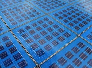
Chemistry professor Jiwoong Park has won a $120,000 award over two years from the Camille and Henry Dreyfus Foundation to support a postdoctoral fellow who will help develop advanced photovoltaic materials at the University’s Institute for Molecular Engineering and Department of Chemistry. Park selected Yu Zhong, who just finished his doctorate in chemistry at Columbia University, for the fellowship.
Solar energy is one of the most promising ways to replace fossil fuels, thereby reducing pollution and minimizing climate change, Park said. “This award will be used to develop new materials and architecture for high-performance hybrid solar cells in the form of economical, detachable, lightweight photovoltaic films.”
The materials will utilize semiconductors that are only one atom thick and will therefore be especially suited for photovoltaic materials that will power nanomachines, such as sensors and detectors.
“When miniaturizing machines, a current limitation is the size of the power source,” Park said. “The thin photovoltaic materials that we will develop will be foldable, like an umbrella. They will be very small when folded but larger when open.”
Such nanomachines would have many applications, he added. “For example, imagine sending thousands of them into the air to gather data about crops or the weather.”
To achieve this, the researchers will synthesize, functionalize and stack atomically thin semiconductors called transition-metal dichalcogenides (TMD), along with other components, into photovoltaic material. The new material will have unique mechanical and electrical characteristics that broaden the application of solar cells and improve their performance, the researchers say.
Their work will combine two active and competitive fields of research: inorganic TMDs, for which Park is renowned, and organic photovoltaics. The former provides a flexible matrix and the latter provides a method for doping the material, which refers to the deliberate, controlled introduction of impurities to semiconductors as a way to alter their mechanical and electrical properties.
“While the layers of TMDs will provide a solid-state material that acts like a platform with advanced physical properties, the organic photovoltaic molecules will provide additional functionalities and allow for direct tuning of the hybrid material’s doping and magnetic fields,” Park said.
“These detachable solar cells will chart a new path to economical, reusable photovoltaic devices for renewable energy sources,” he added.
“There is a great untapped potential in bridging TMDs enhanced with organic photovoltaic materials,” Zhong said. “In order to make hybrid solar cells from these materials, we need to chemically functionalize the materials. My background in organic chemistry and solar cells made me suitable for this work.”
Zhong will be the first fellow in Park’s group of four postdoctoral scholars and six graduate students, all of whom have moved from Cornell University to the University of Chicago.
“There are many opportunities and possibilities in the overlapping realm of inorganic TMDs and organic materials, and the University of Chicago, with its interdisciplinary environment, is a great place to explore these ideas,” Zhong concluded.
The Camille and Henry Dreyfus Foundation is a nonprofit organization devoted to the advancement of chemical sciences. This is the University’s seventh Dreyfus postdoctoral fellowship.
Share on:


Testimonial
"We’re proud to call I-Connect007 a trusted partner. Their innovative approach and industry insight made our podcast collaboration a success by connecting us with the right audience and delivering real results."
Julia McCaffrey - NCAB GroupSuggested Items
Curing and Verification in PCB Shadow Areas
09/17/2025 | Doug Katze, DymaxDesign engineers know a simple truth that often complicates electronics manufacturing: Light doesn’t go around corners. In densely populated PCBs, adhesives and coatings often fail to fully cure in shadowed regions created by tall ICs, connectors, relays, and tight housings.
Marcy’s Musings: Advancing the Advanced Materials Discussion
09/17/2025 | Marcy LaRont -- Column: Marcy's MusingsAs the industry’s most trusted global source of original content about the electronics supply chain, we continually ask you about your concerns, what you care about, and what you most want to learn about. Your responses are insightful and valuable. Thank you for caring enough to provide useful feedback and engage in dialogue.
September 2025 PCB007 Magazine: The Future of Advanced Materials
09/16/2025 | I-Connect007 Editorial TeamMoore’s Law is no more, and the advanced material solutions being developed to grapple with this reality are surprising, stunning, and perhaps a bit daunting. Buckle up for a dive into advanced materials and a glimpse into the next chapters of electronics manufacturing.
I-Connect007 Launches Advanced Electronics Packaging Digest
09/15/2025 | I-Connect007I-Connect007 is pleased to announce the launch of Advanced Electronics Packaging Digest (AEPD), a new monthly digital newsletter dedicated to one of the most critical and rapidly evolving areas of electronics manufacturing: advanced packaging at the interconnect level.
Panasonic Industry will Double the Production Capacity of MEGTRON Multi-layer Circuit Board Materials Over the Next Five Years
09/15/2025 | Panasonic Industry Co., Ltd.Panasonic Industry Co., Ltd., a Panasonic Group company, announced plans for a major expansion of its global production capacity for MEGTRON multi-layer circuit board materials today. The company plans to double its production over the next five years to meet growing demand in the AI server and ICT infrastructure markets.