


 The Marketing Minute: Cracking the Code of Technical Marketing
 Trouble in Your Tank: Implementing Direct Metallization in Advanced Substrate Packaging


3D Solutions to Energy Savings in Silicon Power Transistors
December 7, 2016 | Tokyo Institute of TechnologyEstimated reading time: 2 minutes
In electronics, lower power consumption leads to operation cost savings, environmental benefits and the convenience advantages from longer running devices. While progress in energy efficiencies has been reported with alternative materials such as SiC and GaN, energy-savings in the standard inexpensive and widely used silicon devices are still keenly sought.
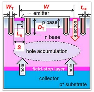
Trench gate IGBT schematic indicating the mesa width (S), gate length (Lg), and the oxide thickness in the MOSFET (tox), cell pitch (W), and the trench depth (DT).
K Tsutsui at Tokyo Institute of Technology and colleagues in Japan have now shown that by scaling down size parameters in all three dimensions their device they can achieve significant energy savings ("Experimental verification of a 3D scaling principle for low Vce(sat) IGBT", Technical Digest of IEDM2016, Session 10.6, (2016), 2016 IEEE International Electron Devices Meeting).
Tsutsui and colleagues studied silicon insulated gate bipolar transistors (IGBTs), a fast-operating switch that features in a number of every day appliances. While the efficiency of IGBTs is good, reducing the ON resistance, or the voltage from collector to emitter required for saturation (Vce(sat)), could help increase the energy efficiency of these devices further.
Previous investigations have highlighted that increases in the "injection enhancement (IE) effect", which give rise to more charge carriers, leads to a reduction in Vce(sat). Although this has been achieved by reducing the mesa width in the device structure, the mesa resistance was thereby increased as well. Reducing the mesa height could help counter the increased resistance but is prone to impeding the (IE) effect. Instead the researchers reduced the mesa width, gate length, and the oxide thickness in the MOSFET to increase the IE effect and so reduce Vce(sat) from 1.70 to 1.26 V. With these alterations the researchers also used a reduced gate voltage, which has advantages for CMOS integration.
They conclude, "It was experimentally confirmed for the first time that significant Vce(sat) reduction can be achieved by scaling the IGBT both in the lateral and vertical dimensions with a decrease in the gate voltage."
Background
Insulated gate bipolar transistors (IGBTs)
These are three terminal devices used as switches or rectifiers. With simple gate-drive characteristics and high-current and low-saturation-voltage capabilities they combine the benefits of two other types of transistors - metal-oxide-semiconductor field effect transistors (MOSFETs) and bipolar transistors.
3D scaling of IGBTs
The researchers reduced the mesa width, gate length, and the oxide thickness in the MOSFET by a factor of 1/k, and compared devices with values of 1 and 3 for k. Because the fabrication of narrow mesas can cause problems they also reduced the trench depth by 1/k. Although this has a slightly negative effect on the IE effect, it has considerable benefits for fabrication ease and cost and the dependence of (Vce(sat)) on the trench depth was deemed to be small. The gate voltage was also decreased by a factor of 1/k, while the cell pitch was maintained at 16 µm.
Share on:


Testimonial
"The I-Connect007 team is outstanding—kind, responsive, and a true marketing partner. Their design team created fresh, eye-catching ads, and their editorial support polished our content to let our brand shine. Thank you all! "
Sweeney Ng - CEE PCBSuggested Items
Alternative Manufacturing, Inc. (AMI) Announces Commitment to Excellence in Industrial, Defense, Aerospace, Renewables, and Robotics Markets
09/16/2025 | Alternative Manufacturing, Inc.Alternative Manufacturing, Inc. (AMI), a 100% employee-owned contract manufacturer, proudly reaffirms its leadership in the electronics manufacturing services (EMS) industry with a continued commitment to delivering high-quality PCBAs and box builds across the industrial, defense, aerospace, renewable energy, and robotics markets.
Elementary Mr. Watson: Running the Signal Gauntlet
09/11/2025 | John Watson -- Column: Elementary, Mr. WatsonIf you’ve ever run a military obstacle course, you know it’s less “fun fitness challenge” and more “how can we inflict as much pain in the shortest time possible?” You start fresh—chest out, lungs full of confidence, thinking you might even look good doing this—and 10 seconds later, you’re questioning all your life choices.
Hitachi Unveils $1B U.S. Investment in Critical Grid Infrastructure
09/05/2025 | Hitachi EnergyHitachi Energy, a wholly owned subsidiary of Hitachi, Ltd., and global leader in electrification, today announced a historic investment of more than $1 billion USD to expand the production of critical electrical grid infrastructure in the United States.
Ferric Launches New Integrated Voltage Regulator for AI and High-Performance Processors
08/27/2025 | BUSINESS WIREFe1766 delivers an unprecedented 160 A in the industry’s smallest IVR footprint, redefining chip-level and system-level power delivery for the AI era.
Tigo Energy Initiates ‘Made in the USA’ Manufacturing Partnership With EG4 Electronics Share
08/27/2025 | BUSINESS WIRETigo Energy, Inc announced a manufacturing and marketing partnership with EG4 Electronics to produce Tigo optimized inverters and Module Level Power Electronics (MLPE) together with EG4 solar inverters in the United States of America.