


 The Marketing Minute: Cracking the Code of Technical Marketing
 Trouble in Your Tank: Implementing Direct Metallization in Advanced Substrate Packaging


Electron Highway Inside Crystal
December 9, 2016 | University of WürzburgEstimated reading time: 4 minutes
Physicists at the University of Würzburg have made an astonishing discovery in a specific type of topological insulators. The effect is due to the structure of the materials used. The researchers have now published their work in the journal Science ("Robust spin-polarized midgap states at step edges of topological crystalline insulators").
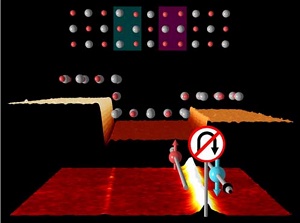
Step edges on topological crystalline insulators may lead to electrically conducting pathways where electrons with opposite spin spin move in converse directions -- any U-turn is prohibited. (Image: Thomas Bathon/Paolo Sessi/Matthias Bode)
Topological insulators are currently the hot topic in physics according to the newspaper Neue Zürcher Zeitung. Only a few weeks ago, their importance was highlighted again as the Royal Swedish Academy of Sciences in Stockholm awarded this year's Nobel Prize in Physics to three British scientists for their research of so-called topological phase transitions and topological phases of matter.
Topological insulators are also being studied at the Departments for Experimental Physics II and Theoretical Physics I of the University of Würzburg. However, they focus on a special version of insulators called topological crystalline insulators (TCI). In cooperation with the Polish Academy of Sciences in Warsaw and the University of Zurich, Würzburg physicists have now achieved a major breakthrough. They were able to detect new electronic states of matter in these insulators.
Step edges direct electrons
The central result: When crystalline materials are split, small atomically flat terraces emerge at the split off surfaces which are separated from each other by step edges. Inside these structures, conductive channels for electrical currents form which are extremely narrow at just about 10 nm and surprisingly robust against external disturbance. Electrons travel on these conductive channels with different spin in opposite directions - similar to a motorway with separate lanes for the two directions. This effect makes the materials interesting for technological applications in future electronic components such as ultra-fast and energy-efficient computers.
"TCIs are relatively simple to produce and they are already different from conventional materials because of their special crystalline structure," Dr. Paolo Sessi explains the background of the recently published paper. Sessi is a research fellow at the Department of Experimental Physics II and the lead author of the study.
Moreover, these materials owe their special quality to their electronic properties: In topological materials, the direction of spin determines the direction in which the electrons travel. Simply put, the "spin" can be interpreted as a magnetic dipole that can point in two directions ("up" and "down"). Accordingly, up-spin electrons in TCIs move in one and down-spin electrons in the other direction.
It's all about the number of atomic layers
"But previously scientists didn't know how to produce the conductive channels required to this end," says Professor Matthias Bode, Head of the Department for Experimental Physics II and co-author of the study. It was chance that now got the researchers on the right track: They discovered that very narrow conductive channels occur naturally when splitting lead tin selenide (PbSnSe), a crystalline insulator.
Step edges on the fragments' surfaces cause this phenomenon. They can be imaged using a high-resolution scanning tunnelling microscopy, or more precisely, the height of the corresponding step edges. "Edges that bridge an even number of atomic layers are totally inconspicuous. But if the edges span an odd number of atomic layers, a small area about 10 nm in width is created that has the electronic conductive channels properties we were looking for," Sessi explains.
Pattern breaks off at the edge
Supported by their colleagues from the Department of Theoretical Physics I and the University of Zurich, the experimental physicists were able to shed light on the origin of these new electronic states. To understand the principle, a little spatial sense is required:
"The crystalline structure causes a layout of the atoms where the different elements alternate like the black and white squares on a chessboard," Matthias Bode explains. This alternating black-and-white pattern applies to both squares which are adjacent and squares situated below and on top one another.
So if the crack of this crystal runs through different atomic layers, more than one edge is created there. Seen from above, white squares may also abut to other white squares along this edge and black squares to other black squares - or identical atoms to identical atoms. However, this only works if an odd number of atomic layers is responsible for the difference in height of the two surfaces.
Backed by calculations
"Calculations show that this offset at the surface is actually causative of these novel electronic states," says Paolo Sessi. Furthermore, they prove that the phenomenon of the spin-dependent conductive channels, which is characteristic of topological materials, occurs here as well.
According to the scientists, this property in particular makes the discovery relevant for potential applications, because such conductive channels cause low conduction loss on the one hand and can be used directly to transmit and process information in the field of spintronics on the other.
However, several questions need to be answered and challenges to be overcome before this will become reality. For instance, the scientists are not yet sure over which distances the currents in the newly discovered conductive channels can be transported. Also, in order to be implemented in circuits, methods would have to be developed that allow creating step edges of a defined height along specified directions.
Share on:


Testimonial
"In a year when every marketing dollar mattered, I chose to keep I-Connect007 in our 2025 plan. Their commitment to high-quality, insightful content aligns with Koh Young’s values and helps readers navigate a changing industry. "
Brent Fischthal - Koh YoungSuggested Items
Curing and Verification in PCB Shadow Areas
09/17/2025 | Doug Katze, DymaxDesign engineers know a simple truth that often complicates electronics manufacturing: Light doesn’t go around corners. In densely populated PCBs, adhesives and coatings often fail to fully cure in shadowed regions created by tall ICs, connectors, relays, and tight housings.
Marcy’s Musings: Advancing the Advanced Materials Discussion
09/17/2025 | Marcy LaRont -- Column: Marcy's MusingsAs the industry’s most trusted global source of original content about the electronics supply chain, we continually ask you about your concerns, what you care about, and what you most want to learn about. Your responses are insightful and valuable. Thank you for caring enough to provide useful feedback and engage in dialogue.
September 2025 PCB007 Magazine: The Future of Advanced Materials
09/16/2025 | I-Connect007 Editorial TeamMoore’s Law is no more, and the advanced material solutions being developed to grapple with this reality are surprising, stunning, and perhaps a bit daunting. Buckle up for a dive into advanced materials and a glimpse into the next chapters of electronics manufacturing.
I-Connect007 Launches Advanced Electronics Packaging Digest
09/15/2025 | I-Connect007I-Connect007 is pleased to announce the launch of Advanced Electronics Packaging Digest (AEPD), a new monthly digital newsletter dedicated to one of the most critical and rapidly evolving areas of electronics manufacturing: advanced packaging at the interconnect level.
Panasonic Industry will Double the Production Capacity of MEGTRON Multi-layer Circuit Board Materials Over the Next Five Years
09/15/2025 | Panasonic Industry Co., Ltd.Panasonic Industry Co., Ltd., a Panasonic Group company, announced plans for a major expansion of its global production capacity for MEGTRON multi-layer circuit board materials today. The company plans to double its production over the next five years to meet growing demand in the AI server and ICT infrastructure markets.