


 The Marketing Minute: Cracking the Code of Technical Marketing
 Trouble in Your Tank: Implementing Direct Metallization in Advanced Substrate Packaging


New Material a Breakthrough for Magnetic Data Storage
December 13, 2016 | CORDISEstimated reading time: 2 minutes
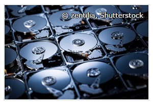
The amount of data generated on a daily basis is quickly surpassing the storage capabilities of today’s hard drives. In order to keep up, the next generation of hard drives must use materials with magnetic properties capable of being easily manipulated, thus offering higher density and better efficiency.
To meet this demand, two EU-funded research projects have developed just such a material. The new perovskite material features a magnetic order that can be easily changed with heat and without causing a disruption to the material itself.
A modified material
Many energy researchers view perovskite photovoltaics as a cheaper alternative to traditional silicon-based systems. However, unlike other forms of perovskite material, the modified version co-created by the TOPOMAT and PICOPROP projects exhibits unique properties that make it the material of choice for the next generation of hard drives.
The TOPOMAT project laid the foundation with its research into the link between the fundamental physical properties of topological insulators and their prospective technological applications. Topological insulators are a recently discovered class of materials that have a bulk electronic gap and exhibit conducting surface states. The PICOPROP project, on the other hand, specifically focuses on the characteristics of the newly discovered perovskite material. Combined, this research – all of which is being conducted at Switzerland’s Ecole Polytechnique Federale de Lausanne (EPFL) – led researchers to discover that, because the new material’s magnetic properties can be easily modified, it is essentially the first magnetic photoconductor.
A combination of properties
This characteristic represents an important breakthrough in the field of magnetic data storage. As a material’s magnetism comes from the interactions of its localised and moving electrons, the result is a fixed magnetic state. The only way to change this state is to alter the structure of the electrons found in the material’s chemistry or crystal structure. However, such a change impacts the makeup of the material itself, thus severely limiting its use for magnetic data storage purposes.
According to an article published in the journal ‘Nature’, the new perovskite material gets around this limitation by combining the advantages of ferromagnets, whose magnetic moments are aligned in a well-defined order, with photoconductors, where light illumination generates high density free conduction electrons.
It is this combination of properties that allows for the melting of magnetisation by photo-electrons (i.e., electrons emitted from material when hit by light). The result is that even a weak light such as a red LED is sufficient to melt the material’s magnetic order, creating a high density of travelling electrons. These electrons can then be easily, quickly and continuously manipulated by simply changing the intensity of the light.
Influential in next-gen hard drives
Although the projects remain a work in progress, these initial results indicate that this new material will prove influential in the creation of next generation high capacity, low energy hard drives. According to one researcher, the perovskite material is the key to combining the advantages of magnetic storage – long-term stability, high data density, non-volatile operation and the ability to rewrite – with the speed of optical writing and reading.
Share on:


Testimonial
"We’re proud to call I-Connect007 a trusted partner. Their innovative approach and industry insight made our podcast collaboration a success by connecting us with the right audience and delivering real results."
Julia McCaffrey - NCAB GroupSuggested Items
Curing and Verification in PCB Shadow Areas
09/17/2025 | Doug Katze, DymaxDesign engineers know a simple truth that often complicates electronics manufacturing: Light doesn’t go around corners. In densely populated PCBs, adhesives and coatings often fail to fully cure in shadowed regions created by tall ICs, connectors, relays, and tight housings.
Marcy’s Musings: Advancing the Advanced Materials Discussion
09/17/2025 | Marcy LaRont -- Column: Marcy's MusingsAs the industry’s most trusted global source of original content about the electronics supply chain, we continually ask you about your concerns, what you care about, and what you most want to learn about. Your responses are insightful and valuable. Thank you for caring enough to provide useful feedback and engage in dialogue.
September 2025 PCB007 Magazine: The Future of Advanced Materials
09/16/2025 | I-Connect007 Editorial TeamMoore’s Law is no more, and the advanced material solutions being developed to grapple with this reality are surprising, stunning, and perhaps a bit daunting. Buckle up for a dive into advanced materials and a glimpse into the next chapters of electronics manufacturing.
I-Connect007 Launches Advanced Electronics Packaging Digest
09/15/2025 | I-Connect007I-Connect007 is pleased to announce the launch of Advanced Electronics Packaging Digest (AEPD), a new monthly digital newsletter dedicated to one of the most critical and rapidly evolving areas of electronics manufacturing: advanced packaging at the interconnect level.
Panasonic Industry will Double the Production Capacity of MEGTRON Multi-layer Circuit Board Materials Over the Next Five Years
09/15/2025 | Panasonic Industry Co., Ltd.Panasonic Industry Co., Ltd., a Panasonic Group company, announced plans for a major expansion of its global production capacity for MEGTRON multi-layer circuit board materials today. The company plans to double its production over the next five years to meet growing demand in the AI server and ICT infrastructure markets.