


 The Marketing Minute: Cracking the Code of Technical Marketing
 Trouble in Your Tank: Implementing Direct Metallization in Advanced Substrate Packaging


Lightning-Fast Switch for Electron Waves
December 13, 2016 | Universität RegensburgEstimated reading time: 2 minutes
The characteristic shine of metals is created by electrons which can freely move in the interior of the material and reflect incoming radiation. Similar to water waves on a pond, waves can form on the surface of this electron sea – so called “surface plasmons”. Instead of a stone that is thrown into water, light is used to generate surface plasmons in the laboratory. When light is focused onto a nanometer-sharp metallic tip, miniature waves propagate on the material’s surface in a circular fashion starting from the tip apex. A nanometer is only approximately ten times the size of the diameter of a single atom. The miniature waves could be used in future compact electronic devices for lightning-fast information transport.
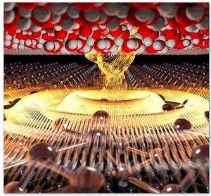
In the heterostructure, waves of the plasma on black phosphorus (lower part) expand starting from the point of their excitation and cause the adjacent silicon dioxide (upper part) to oscillate. (Image: Fabian Mooshammer)
So far, however, there has been no means of switching such surface waves on and off on ultrafast timescales, which is essential. Conversely, in conventional electronics the analogous mechanism is realized by transistors.
Now, for the first time, a team of scientists at the University of Regensburg, in collaboration with colleagues from Pisa, have demonstrated the experimental on/off switching of waves on the electron sea, laying the foundation for future plasma-electronics (Nature Nanotechnology, "Femtosecond photo-switching of interface polaritons in black phosphorus heterostructures").
The key was that the physicists did not use a metal, where electron waves are always present. Instead a much more sophisticated heterostructure based on a semiconductor was developed by Miriam S. Vitiello and colleagues from Pisa for the study.
Semiconductors like, for example, silicon are the materials from which computer chips are made. The semiconductor in this heterostructure is an especially modern material: so-called “black phosphorus”. Upon irradiation by intense light pulses, freely moving electrons are generated inside the material. Without these electrons, no surface waves are present and the structure is switched “off”. However, as soon as the first laser pulse generates the free electrons, a subsequent pulse can start the propagation of surface plasmons from the tip.
To test how fast this switching process can take place, the team of Prof. Dr. Rupert Huber in Regensburg activated surface plasmons with ultrafast laser pulses that were as short as a few femtoseconds. One femtosecond is the unimaginably short time span of the millionth part of a billionth of a second, i.e. 0, 000 000 000 000 001 seconds.
Employing their worldwide unique microscope featuring nanometer spatial resolution in addition to ultrafast temporal resolution, the scientists subsequently traced the expansion of the plasmon waves in extreme slow motion snapshots. In this process it was clearly visible that the switching times where on the femtosecond scale, and thus many orders of magnitude faster than the fastest existing transistors.
As a pleasant surprise it was also found, that the wavelength of the surface waves is almost independent of the power of the laser which switches the structure.
These results are highly encouraging for future ultrafast electronics based on surface plasmons. In the next step, the scientists from Regensburg are testing first operational plasmonic components – on femtosecond time scales.
Share on:


Testimonial
"Advertising in PCB007 Magazine has been a great way to showcase our bare board testers to the right audience. The I-Connect007 team makes the process smooth and professional. We’re proud to be featured in such a trusted publication."
Klaus Koziol - atgSuggested Items
Driving Innovation: Depth Routing Processes—Achieving Unparalleled Precision in Complex PCBs
09/08/2025 | Kurt Palmer -- Column: Driving InnovationIn PCB manufacturing, the demand for increasingly complex and miniaturized designs continually pushes the boundaries of traditional fabrication methods, including depth routing. Success in these applications demands not only on robust machinery but also sophisticated control functions. PCB manufacturers rely on advanced machine features and process methodologies to meet their precise depth routing goals. Here, I’ll explore some crucial functions that empower manufacturers to master complex depth routing challenges.
Polar Instruments Announces Additive Transmission Line Support for Si9000e
08/20/2025 | Polar InstrumentsTransmission lines embedded into the PCB surface are a feature of UHDI constructions. The 2025 fall release of Polar's Si9000e PCB impedance & insertion loss transmission line field solver incorporates eight new single ended, differential and coplanar transmission line structures.
Henniker Plasma Launches Stratus Turnkey Plasma Manufacturing Cell
08/13/2025 | Henniker PlasmaHenniker Plasma, a leading manufacturer of plasma treatment systems, proudly announces the launch of its Stratus Plasma Manufacturing Cell range — a fully integrated, turnkey solution that combines advanced atmospheric plasma surface treatment with robotic automation.
Trouble in Your Tank: Metallizing Flexible Circuit Materials—Mitigating Deposit Stress
08/04/2025 | Michael Carano -- Column: Trouble in Your TankMetallizing materials, such as polyimide used for flexible circuitry and high-reliability multilayer printed wiring boards, provide a significant challenge for process engineers. Conventional electroless copper systems often require pre-treatments with hazardous chemicals or have a small process window to achieve uniform coverage without blistering. It all boils down to enhancing the adhesion of the thin film of electroless copper to these smooth surfaces.
Designers Notebook: Basic PCB Planning Criteria—Establishing Design Constraints
07/22/2025 | Vern Solberg -- Column: Designer's NotebookPrinted circuit board development flows more smoothly when all critical issues are predefined and understood from the start. As a basic planning strategy, the designer must first consider the product performance criteria, then determine the specific industry standards or specifications that the product must meet. Planning also includes a review of all significant issues that may affect the product’s manufacture, performance, reliability, overall quality, and safety.