


 The Marketing Minute: Cracking the Code of Technical Marketing
 Trouble in Your Tank: Implementing Direct Metallization in Advanced Substrate Packaging


New Properties Discovered in Atom-Wide Troughs
December 15, 2016 | U.S. Department of EnergyEstimated reading time: 1 minute
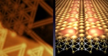
Could adding defects make a good material even better? Scientists have found that linear defects in a promising thin film create one-atom-thick metallic wires. These wires cross the otherwise intact material, offering a way to channel electrons and photons, tiny packets of light. A multidisciplinary team made this discovery using resources at the Molecular Foundry and the Advanced Light Source.
The team worked with transition metal dichalcogenides (TMDs) because the materials have exceptional optical characteristics. This research found that a single TMD layer could emit as much light as an equivalent material that is 10,000 times thicker, paving the way toward smaller, more efficient devices. Further, the team found that engineering defects (purposely introducing missing or displaced atoms) into TMDs could modify their intrinsic properties. These modifications might improve the material or lead to altogether new useful properties for future energy conversion, quantum computing and communication systems.
In the world of semiconductors, impurities and defects can be a good thing. They modify the properties of materials such as silicon, and scientists can exploit these properties to develop better transistors for laptop computers, smart phones, and solar cells. Recently, scientists discovered a new class of semiconductor that is only three atoms thick and extends in a two-dimensional plane, similar to graphene. These two-dimensional semiconductors, called transition metal dichalcogenides (TMDs), have exceptional optical characteristics. They can be developed into ultra-sensitive photodetectors, and a single TMD layer emits as much light as a three-dimensional TMD crystal composed of 10,000 layers.
For the past several years, scientists have wondered if impurities and defects could also modify TMDs’ intrinsic properties, perhaps in ways that improve the semiconductor or lead to new functionalities. Scientists at the Molecular Foundry, in collaboration with researchers at the Advanced Light Source, have taken a big step towards answering this question. They found—to their surprise—how substantial linear defects in TMDs create entirely new properties. Some of these properties indicate that defects in TMDs might even mediate superconducting states.
The team synthesized three-atom-thick, clean layers of molybdenum diselenide, which is a type of TMD. They then studied the material with a microscope that can visualize atoms and their electronic wave functions. They discovered a linear defect formed by a line of missing selenium atoms. This defect creates one-atom-thick metallic wires to transport electrons or photons across the otherwise intact semiconductor like veins.
Share on:


Testimonial
"In a year when every marketing dollar mattered, I chose to keep I-Connect007 in our 2025 plan. Their commitment to high-quality, insightful content aligns with Koh Young’s values and helps readers navigate a changing industry. "
Brent Fischthal - Koh YoungSuggested Items
Curing and Verification in PCB Shadow Areas
09/17/2025 | Doug Katze, DymaxDesign engineers know a simple truth that often complicates electronics manufacturing: Light doesn’t go around corners. In densely populated PCBs, adhesives and coatings often fail to fully cure in shadowed regions created by tall ICs, connectors, relays, and tight housings.
Marcy’s Musings: Advancing the Advanced Materials Discussion
09/17/2025 | Marcy LaRont -- Column: Marcy's MusingsAs the industry’s most trusted global source of original content about the electronics supply chain, we continually ask you about your concerns, what you care about, and what you most want to learn about. Your responses are insightful and valuable. Thank you for caring enough to provide useful feedback and engage in dialogue.
September 2025 PCB007 Magazine: The Future of Advanced Materials
09/16/2025 | I-Connect007 Editorial TeamMoore’s Law is no more, and the advanced material solutions being developed to grapple with this reality are surprising, stunning, and perhaps a bit daunting. Buckle up for a dive into advanced materials and a glimpse into the next chapters of electronics manufacturing.
I-Connect007 Launches Advanced Electronics Packaging Digest
09/15/2025 | I-Connect007I-Connect007 is pleased to announce the launch of Advanced Electronics Packaging Digest (AEPD), a new monthly digital newsletter dedicated to one of the most critical and rapidly evolving areas of electronics manufacturing: advanced packaging at the interconnect level.
Panasonic Industry will Double the Production Capacity of MEGTRON Multi-layer Circuit Board Materials Over the Next Five Years
09/15/2025 | Panasonic Industry Co., Ltd.Panasonic Industry Co., Ltd., a Panasonic Group company, announced plans for a major expansion of its global production capacity for MEGTRON multi-layer circuit board materials today. The company plans to double its production over the next five years to meet growing demand in the AI server and ICT infrastructure markets.