


 The Marketing Minute: Cracking the Code of Technical Marketing
 Trouble in Your Tank: Implementing Direct Metallization in Advanced Substrate Packaging


Innovations Offer Peek Into the Future of Electronic Devices
December 15, 2016 | Purdue UniversityEstimated reading time: 4 minutes
Purdue University researchers - during the international IEDM 2016 conference the week of Dec. 5 - showcased a range of concepts and technologies that foreshadow the future of the semiconductor industry.
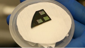
Purdue University researchers recently showcased a range of concepts and technologies that foreshadow the future of the semiconductor industry. Here, a device is made from the semiconductor germanium, in research led by Peide Ye, Purdue's Richard J. and Mary Jo Schwartz Professor of Electrical and Computer Engineering. (Purdue University image/Erin Easterling)
The concepts included innovations to extend the performance of today's silicon-based transistors, along with entirely new types of nanoelectronic devices to complement and potentially replace conventional technology in future computers.
"For the past 50 years, ever more electronic devices envelop us in our day-to-day life, and electronic-device innovation has been a major economic factor in the U.S. and world economy," said Gerhard Klimeck, a professor of electrical and computer engineering and director of Purdue's Network for Computational Nanotechnology in the university's Discovery Park. "These advancements were enabled by making the basic transistors in computer chips ever smaller. Today the critical dimensions in these devices are just some 60 atoms thick, and further device size reductions will certainly stop at small atomic dimensions."
New technologies will be needed for industry to keep pace with Moore's law, an observation that the number of transistors on a computer chip doubles about every two years, resulting in rapid progress in computers and telecommunications. It is becoming increasingly difficult to continue shrinking electronic devices made of conventional silicon-based semiconductors, called complementary metal-oxide-semiconductor (CMOS) technology, said Muhammad Ashraful Alam, Purdue University's Jai N. Gupta Professor of Electrical and Computer Engineering.
“As transistors are becoming smaller they are facing a number of challenges in terms of increasing their performance and ensuring their reliability,” he said.
Purdue researchers presented five papers proposing innovative designs to extend CMOS technology and new devices to potentially replace or augment conventional transistors during the annual International Electron Devices Meeting (IEDM 2016) Dec. 5-7 in San Francisco. The conference showcases the latest developments in electronic device technology.
Integrated circuits, or chips, now contain around 2 billion transistors. The more devices that are packed onto a chip, the greater the heating, with today’s chips generating around 100 watts per square centimeter, comparable to that of a nuclear reactor.
"As a result, self-heating has become a fundamental concern that hinders performance and can damage transistors, and we are making advances to address it," Alam said.
Two of the IEDM conference papers detail research to suppress self-heating and enhance the performance of conventional CMOS chips. The remaining papers deal with new devices for future computer technologies that require lower power to operate, meaning they would not self-heat as significantly.
"We are not only working to extend the state-of-art of traditional technology, but also to develop next-generation transistor technologies," Alam said.
Transistors are electronic switches that turn on and off to allow computations using the binary code of ones and zeros. A critical component in transistors, called the gate, controls this switching. As progressively smaller transistors are designed, however, this control becomes increasingly difficult because electrons leak around the ultra-small gate.
One of the conference papers focuses on a potential solution to this leakage: creating transistors that are surrounded by the gate, instead of the customary flat design. Unfortunately, enveloping the transistor with a gate causes increased heating, which hinders reliability and can damage the device. The researchers used a technique called submicron thermo-reflectance imaging to pinpoint locations of excessive heating. Another paper details a potential approach to suppress this self-heating, modeling how to more effectively dissipate heat by changing how the transistor connects to the complex circuitry in the chip.
The three remaining papers propose next-generation devices: networks of nanomagnets, extremely thin layers of a material called black phosphorous and "tunnel" field effect transistors, or FETs. Such technologies would operate at far lower voltages than existing electronics, generating less heat.
"You want to use as low a voltage as possible because that reduces power dissipation and if you can reduce power dissipation the battery of your cell phone will last longer, you can do more computing with a smaller amount of power and you will be able to cram more functional elements into a given area," Klimeck said.
The tunnel FETS could potentially reduce power consumption by more than 40 times.
"Reducing power consumption by a factor of 40 would be a huge development," Klimeck said.
Another conference paper details research to develop devices made of black phosphorous, which might one day replace silicon as a semiconductor in transistors. Findings showed the devices can pass large amounts of current with ultra-low resistance while demonstrating good switching performance, said Peide Ye, the Richard J. and Mary Jo Schwartz Professor of Electrical and Computer Engineering.
"We have demonstrated the highest performance of this kind of 2-D device," Ye said.
Devices made from the material also could bring new types of optical and chemical sensors. The devices were created using a technique called chemical vapor deposition in research performed at Purdue's Birck Nanotechnology Center.
Future research will include efforts to create smaller black phosphorous devices, Ye said.
A fifth paper details how networks of nanomagnets could serve as the building blocks of future computers. Findings show the networks mimic Ising networks - named after German physicist Ernst Ising - which harness mathematics to solve complex probabilistic problems.
The nanomagnet networks might be used to draw from huge databases to perform demanding jobs in areas ranging from business and finance, to health care and scientific research.
The conventional approach to performing big data computations is through new software running on CMOS devices. However, nanomagnet networks represent a different approach: developing an entirely new type of hardware for the feat, said Zhihong Chen, an associate professor of electrical and computer engineering.
"We have shown experimentally that the nanomagnet arrays are potential building blocks for probabilistic computer hardware," Chen said.
Share on:


Testimonial
"We’re proud to call I-Connect007 a trusted partner. Their innovative approach and industry insight made our podcast collaboration a success by connecting us with the right audience and delivering real results."
Julia McCaffrey - NCAB GroupSuggested Items
Meet the Author Podcast: Martyn Gaudion Unpacks the Secrets of High-Speed PCB Design
07/16/2025 | I-Connect007In this special Meet the Author episode of the On the Line with… podcast, Nolan Johnson sits down with Martyn Gaudion, signal integrity expert, managing director of Polar Instruments, and three-time author in I-Connect007’s popular The Printed Circuit Designer’s Guide to... series.
Intervala Hosts Employee Car and Motorcycle Show, Benefit Nonprofits
08/27/2024 | IntervalaIntervala hosted an employee car and motorcycle show, aptly named the Vala-Cruise and it was a roaring success! Employees had the chance to show off their prized wheels, and it was incredible to see the variety and passion on display.
KIC Honored with IPC Recognition for 25 Years of Membership and Contributions to Electronics Manufacturing Industry
06/24/2024 | KICKIC, a renowned pioneer in thermal process and temperature measurement solutions for electronics manufacturing, is proud to announce that it has been recognized by IPC for 25 years of membership and significant contributions to electronics manufacturing.
Boeing Starliner Spacecraft Completes Successful Crewed Docking with International Space Station
06/07/2024 | BoeingNASA astronauts Barry "Butch" Wilmore and Sunita "Suni" Williams successfully docked Boeing's Starliner spacecraft to the International Space Station (ISS), about 26 hours after launching from Cape Canaveral Space Force Station.
KIC’s Miles Moreau to Present Profiling Basics and Best Practices at SMTA Wisconsin Chapter PCBA Profile Workshop
01/25/2024 | KICKIC, a renowned pioneer in thermal process and temperature measurement solutions for electronics manufacturing, announces that Miles Moreau, General Manager, will be a featured speaker at the SMTA Wisconsin Chapter In-Person PCBA Profile Workshop.