


 The Marketing Minute: Cracking the Code of Technical Marketing
 Trouble in Your Tank: Implementing Direct Metallization in Advanced Substrate Packaging


CHESS Facility Helps Scale Up Solar Cells
December 16, 2016 | Cornell UniversityEstimated reading time: 3 minutes
Scientists and engineers are constantly working to improve the performance of solar cells. Rather than changing their formulas by trial and error, they would like to understand the chemistry that happens as their recipes cook.
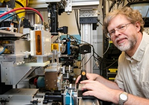
Visiting scientists from the University of Virginia have used the facilities of the Cornell High Energy Synchrotron Source (CHESS) to observe their chemistry in action. By firing high-intensity X-rays into a sample in a process known as X-ray crystallography, CHESS scientists took a series of snapshots of a material as it crystallized, showing how changes in the formula affect the process of crystal growth.
“To be really technologically relevant,” said Joshua Choi, M.Eng. ’07, M.S. ’10, Ph.D. ’12, assistant professor of chemical engineering at the University of Virginia, “we need to be able to scale up this process while maintaining or even improving the efficiency of the solar cell. To do that, we need to understand how this material crystallizes and grows from solution into a thin film.”
A long-range goal, he added, is to be able to move the process from the laboratory to commercial manufacturing.
Choi brought his experiments to Ithaca in collaboration with Paulette Clancy, the Samuel W. and M. Diane Bodman Professor in Chemical Engineering; Blaire Sorenson, a master’s student in Clancy’s research group; and Detlef Smilgies, senior research associate at the Wilson Synchrotron Lab.
Choi works with a new class of materials called “metal halide perovskites,” or MHPs, compounds of lead with chlorine, bromine or iodine, which have aroused recent interest. The performance of recently crafted MHP solar cells rivals conventional silicon solar cells. Dissolved in an organic liquid, MHP materials can be sprayed as a thin film on a glass or silicon substrate, offering an inexpensive way to make large solar collectors. The film also can be deposited on flexible, lightweight materials, making it possible to produce rolls of thin solar cell material that could be applied to houses, cars or wearables.
As the film sprayed on a surface dries, the material crystallizes into an orderly crystal lattice of interconnected atoms. How the crystal is structured can make a big difference in performance, and engineers have found that the choice of solvent or adding some additional reagents can change the structure.
In a series of experiments with several different formulations, CHESS researchers placed newly coated cells in the path of a beam of high-energy X-rays. X-rays passing through a grid of atoms will emerge in a pattern from which the structure of the crystal lattice can be determined. (Ordinary light can’t do this, because its wavelength is longer than the dimensions of atoms so it passes them by without interacting. X-rays have a vastly shorter wavelength.)
A series of snapshots taken every few seconds while the films were drying showed how the crystals formed. The tests showed that using a solvent called tetrahydrothiophene oxide led to more uniform crystal growth and enabled the experimenters to control the orientation of the crystal, which has a major effect on the voltage the cell produces. “These findings” Choi said, “highlight the importance of understanding and controlling the MHP thin film formation processes to rationally improve the performance of solar cells.”
Choi, with University of Virginia doctoral student Justin Girard and undergraduate researcher Benjamin Foley, will present the findings at the 66th meeting of the American Crystallographic Association, July 22-26 in Denver. Choi’s group also collaborated with scientists at Wake Forest University and the University of Pittsburgh on a paper, “Controlling Nucleation, Growth, and Orientation of the Metal Halide Perovskite Thin Films with Rationally Selected Additives,” released in the online edition of the Journal Materials Chemistry A.
CHESS is – almost literally – a “spinoff” of the Cornell Electron Storage Ring (CESR), a synchrotron buried under Upper Alumni Field where electrons circling in a ring a half mile in circumference are accelerated to high energies for experiments in particle physics. When electrons change direction, as in following a curve, they give off some of their energy as X-rays, so-called “synchrotron radiation,” which CHESS taps at 11 experimental stations around the ring. In addition to doing crystallography, the facility has produced incredibly detailed X-ray images of insects and microorganisms, sometimes observing biochemical processes in progress.
It is one of only two high-energy synchrotron sources in the U.S. (the other is the Advanced Photon Source at Argonne National Laboratory) and one of only five in the world. In the last fiscal year, 1,071 visiting researchers conducted 3,243 unique experiments. A significant effort of the staff is aimed at developing synchrotron radiation experimental facilities and methods.
CHESS is supported by grants from the Division of Materials Research of the National Science Foundation. Choi’s research is funded by NASA and the U.S. Department of Energy.
Share on:


Testimonial
"In a year when every marketing dollar mattered, I chose to keep I-Connect007 in our 2025 plan. Their commitment to high-quality, insightful content aligns with Koh Young’s values and helps readers navigate a changing industry. "
Brent Fischthal - Koh YoungSuggested Items
Curing and Verification in PCB Shadow Areas
09/17/2025 | Doug Katze, DymaxDesign engineers know a simple truth that often complicates electronics manufacturing: Light doesn’t go around corners. In densely populated PCBs, adhesives and coatings often fail to fully cure in shadowed regions created by tall ICs, connectors, relays, and tight housings.
Marcy’s Musings: Advancing the Advanced Materials Discussion
09/17/2025 | Marcy LaRont -- Column: Marcy's MusingsAs the industry’s most trusted global source of original content about the electronics supply chain, we continually ask you about your concerns, what you care about, and what you most want to learn about. Your responses are insightful and valuable. Thank you for caring enough to provide useful feedback and engage in dialogue.
September 2025 PCB007 Magazine: The Future of Advanced Materials
09/16/2025 | I-Connect007 Editorial TeamMoore’s Law is no more, and the advanced material solutions being developed to grapple with this reality are surprising, stunning, and perhaps a bit daunting. Buckle up for a dive into advanced materials and a glimpse into the next chapters of electronics manufacturing.
I-Connect007 Launches Advanced Electronics Packaging Digest
09/15/2025 | I-Connect007I-Connect007 is pleased to announce the launch of Advanced Electronics Packaging Digest (AEPD), a new monthly digital newsletter dedicated to one of the most critical and rapidly evolving areas of electronics manufacturing: advanced packaging at the interconnect level.
Panasonic Industry will Double the Production Capacity of MEGTRON Multi-layer Circuit Board Materials Over the Next Five Years
09/15/2025 | Panasonic Industry Co., Ltd.Panasonic Industry Co., Ltd., a Panasonic Group company, announced plans for a major expansion of its global production capacity for MEGTRON multi-layer circuit board materials today. The company plans to double its production over the next five years to meet growing demand in the AI server and ICT infrastructure markets.