


 The Marketing Minute: Cracking the Code of Technical Marketing
 Trouble in Your Tank: Implementing Direct Metallization in Advanced Substrate Packaging


Scientists Design New Heat-Guiding Device That Is Thinner Than Hair
December 27, 2016 | SUTDEstimated reading time: 1 minute
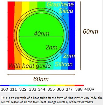
Researchers at Singapore University of Technology and Design (SUTD), University of Bath and University of Cambridge have designed for the first time a heat-guiding structure on the size of nanometers that can steer heat away from, or even towards critical regions of current silicon (or advanced chalcogenide) chips through computer simulations.
Heat guides were formed using graphene and silicon dioxide. Graphene has been previously demonstrated to be an excellent material that allows heat to flow easily along its layers, while silicon dioxide has been shown to be a good medium that resists heat. For example, by stacking these materials together, they can produce an effect of ʹrelative heat flowʹ, making a selected region of silicon or chalcogenide ʹinvisibleʹ to heat.
Co-author, Assistant Professor Desmond Loke from SUTD, said, “Previous research has demonstrated heat-guiding devices showing these effects on the size of micrometers. However, we can now show that this works for structures that are 1,000 times smaller and on silicon or advanced phase-change alloys, making it more useful to remove or keep heat to manufacture tinier electronic devices for current applications, such as smartphones, internet of things (IoT), virtual reality (VR), data centers, etc.”
Using purely heat through such heat-guiding structures, the scientists showed that it was even possible to perform a complete set of ʹBooleanʹ logic operations, and an entire series of ʹspike-timing-dependent plasticityʹ learning processes.
“These heat guides could find widespread uses in more compact integrated circuits for future applications, such as reconfigurable computing, deep learning, artificial intelligence (AI),” Loke added.
This research is funded by a SUTD Temasek Seed grant and published in the journal ACS Applied Materials and Interfaces.
Share on:


Testimonial
"In a year when every marketing dollar mattered, I chose to keep I-Connect007 in our 2025 plan. Their commitment to high-quality, insightful content aligns with Koh Young’s values and helps readers navigate a changing industry. "
Brent Fischthal - Koh YoungSuggested Items
Electra’s ElectraJet EMJ110 Inkjet Soldermask Now in Black & Blue at Sunrise Electronics
09/08/2025 | Electra Polymers LtdFollowing the successful deployment of Electra’s Green EMJ110 Inkjet Soldermask on KLA’s Orbotech Neos™ platform at Sunrise Electronics in Elk Grove Village, Illinois, production has now moved beyond green.
Magnachip Semiconductor Announces YJ Kim to Step Down as CEO; Current Board Chairman Camillo Martino Appointed Interim CEO
08/14/2025 | PR NewswireMagnachip Semiconductor Corporation today announced that YJ Kim has agreed to step down as CEO and as a member of the Board of Directors, effective immediately. Camillo Martino, Chairman of the Board of Directors, has also been appointed Interim Chief Executive Officer, effective immediately.
Bell to Build X-Plane for Phase 2 of DARPA Speed and Runway Independent Technologies (SPRINT) X-Plane Program
07/09/2025 | Bell Textron Inc.Bell Textron Inc., a Textron Inc. company, has been down-selected for Phase 2 of Defense Advanced Research Projects Agency (DARPA) Speed and Runway Independent Technologies (SPRINT) X-Plane program with the objective to complete design, construction, ground testing and certification of an X-plane demonstrator.
Nolan’s Notes: Moving Forward With Confidence
06/03/2025 | Nolan Johnson -- Column: Nolan's NotesWe’re currently enjoying a revitalized and dynamic EMS provider market with significant growth potential. Since December 2024, the book-to-bill has been extremely strong and growing. Starting with a ratio of 1.24 in December, book-to-bill has continued to accelerate to a 1.41 in April. Yet, there is a global economic restructuring taking place. To say that the back-and-forth with tariffs and trade deals makes for an uncertain market is an understatement. While we may be in a 90-day tariff pause among leading economic nations, the deadline is quickly approaching and that leaves many of you feeling unsettled about what to expect.
Mycronic High Flex Changes Division Name to PCB Assembly Solutions
05/20/2025 | MycronicMycronic AB, the leading Sweden-based electronics assembly solutions provider, announced that its division formerly known as High Flex will now operate under the name PCB Assembly Solutions.