


 The Marketing Minute: Cracking the Code of Technical Marketing
 Trouble in Your Tank: Implementing Direct Metallization in Advanced Substrate Packaging


Researchers Use World's Smallest Diamonds to Make Wires Three Atoms Wide
December 28, 2016 | Stanford UniversityEstimated reading time: 4 minutes
Scientists at Stanford University and the Department of Energy’s SLAC National Accelerator Laboratory have discovered a way to use diamondoids – the smallest possible bits of diamond – to assemble atoms into the thinnest possible electrical wires, just three atoms wide.
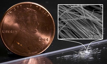
Fuzzy white clusters of nanowires on a lab bench, with a penny for scale. Assembled with the help of diamondoids, the microscopic nanowires can be seen with the naked eye because the strong mutual attraction between their diamondoid shells makes them clump together, in this case by the millions. At top right, an image made with a scanning electron microscope shows nanowire clusters magnified 10,000 times. (SEM image by Hao Yan/SIMES; photo by SLAC National Accelerator Laboratory)
By grabbing various types of atoms and putting them together LEGO-style, the new technique could potentially be used to build tiny wires for a wide range of applications, including fabrics that generate electricity, optoelectronic devices that employ both electricity and light, and superconducting materials that conduct electricity without any loss. The scientists reported their results today in Nature Materials.
“What we have shown here is that we can make tiny, conductive wires of the smallest possible size that essentially assemble themselves,” said Hao Yan, a Stanford postdoctoral researcher and lead author of the paper. “The process is a simple, one-pot synthesis. You dump the ingredients together and you can get results in half an hour. It’s almost as if the diamondoids know where they want to go.”
The Smaller the Better
Although there are other ways to get materials to self-assemble, this is the first one shown to make a nanowire with a solid, crystalline core that has good electronic properties, said study co-author Nicholas Melosh, an associate professor at SLAC and Stanford and investigator with SIMES, the Stanford Institute for Materials and Energy Sciences at SLAC.
The needle-like wires have a semiconducting core – a combination of copper and sulfur known as a chalcogenide – surrounded by the attached diamondoids, which form an insulating shell.
Their minuscule size is important, Melosh said, because a material that exists in just one or two dimensions – as atomic-scale dots, wires or sheets – can have very different, extraordinary properties compared to the same material made in bulk. The new method allows researchers to assemble those materials with atom-by-atom precision and control.
The diamondoids they used as assembly tools are tiny, interlocking cages of carbon and hydrogen. Found naturally in petroleum fluids, they are extracted and separated by size and geometry in a SLAC laboratory. Over the past decade, a SIMES research program led by Melosh and SLAC/Stanford Professor Zhi-Xun Shen has found a number of potential uses for the little diamonds, including improving electron microscope images and making tiny electronic gadgets.
Constructive Attraction
For this study, the research team took advantage of the fact that diamondoids are strongly attracted to each other, through what are known as van der Waals forces. (This attraction is what makes the microscopic diamondoids clump together into sugar-like crystals, which is the only reason you can see them with the naked eye.)
They started with the smallest possible diamondoids – single cages that contain just 10 carbon atoms – and attached a sulfur atom to each. Floating in a solution, each sulfur atom bonded with a single copper ion. This created the basic nanowire building block.
The building blocks then drifted toward each other, drawn by the van der Waals attraction between the diamondoids, and attached to the growing tip of the nanowire.
“Much like LEGO blocks, they only fit together in certain ways that are determined by their size and shape,” said Stanford graduate student Fei Hua Li, who played a critical role in synthesizing the tiny wires and figuring out how they grew. “The copper and sulfur atoms of each building block wound up in the middle, forming the conductive core of the wire, and the bulkier diamondoids wound up on the outside, forming the insulating shell.”
A Versatile Toolkit for Creating Novel Materials
The team has already used diamondoids to make one-dimensional nanowires based on cadmium, zinc, iron and silver, including some that grew long enough to see without a microscope, and they have experimented with carrying out the reactions in different solvents and with other types of rigid, cage-like molecules, such as carboranes.
The cadmium-based wires are similar to materials used in optoelectronics, such as light-emitting diodes (LEDs), and the zinc-based ones are like those used in solar applications and in piezoelectric energy generators, which convert motion into electricity.
“You can imagine weaving those into fabrics to generate energy,” Melosh said. “This method gives us a versatile toolkit where we can tinker with a number of ingredients and experimental conditions to create new materials with finely tuned electronic properties and interesting physics.”
Theorists led by SIMES Director Thomas Devereaux modeled and predicted the electronic properties of the nanowires, which were examined with X-rays at SLAC’s Stanford Synchrotron Radiation Lightsource, a DOE Office of Science User Facility, to determine their structure and other characteristics.
Share on:


Testimonial
"The I-Connect007 team is outstanding—kind, responsive, and a true marketing partner. Their design team created fresh, eye-catching ads, and their editorial support polished our content to let our brand shine. Thank you all! "
Sweeney Ng - CEE PCBSuggested Items
Trouble in Your Tank: Implementing Direct Metallization in Advanced Substrate Packaging
09/15/2025 | Michael Carano -- Column: Trouble in Your TankDirect metallization systems based on conductive graphite are gaining popularity throughout the world. The environmental and productivity gains achievable with this process are outstanding. Direct metallization reduces the costs of compliance, waste treatment, and legal issues related to chemical exposure. A graphite-based direct plate system has been devised to address these needs.
Closing the Loop on PCB Etching Waste
09/09/2025 | Shawn Stone, IECAs the PCB industry continues its push toward greener, more cost-efficient operations, Sigma Engineering’s Mecer System offers a comprehensive solution to two of the industry’s most persistent pain points: etchant consumption and rinse water waste. Designed as a modular, fully automated platform, the Mecer System regenerates spent copper etchants—both alkaline and acidic—and simultaneously recycles rinse water, transforming a traditionally linear chemical process into a closed-loop system.
Driving Innovation: Depth Routing Processes—Achieving Unparalleled Precision in Complex PCBs
09/08/2025 | Kurt Palmer -- Column: Driving InnovationIn PCB manufacturing, the demand for increasingly complex and miniaturized designs continually pushes the boundaries of traditional fabrication methods, including depth routing. Success in these applications demands not only on robust machinery but also sophisticated control functions. PCB manufacturers rely on advanced machine features and process methodologies to meet their precise depth routing goals. Here, I’ll explore some crucial functions that empower manufacturers to master complex depth routing challenges.
Trouble in Your Tank: Minimizing Small-via Defects for High-reliability PCBs
08/27/2025 | Michael Carano -- Column: Trouble in Your TankTo quote the comedian Stephen Wright, “If at first you don’t succeed, then skydiving is not for you.” That can be the battle cry when you find that only small-diameter vias are exhibiting voids. Why are small holes more prone to voids than larger vias when processed through electroless copper? There are several reasons.
The Government Circuit: Navigating New Trade Headwinds and New Partnerships
08/25/2025 | Chris Mitchell -- Column: The Government CircuitAs global trade winds continue to howl, the electronics manufacturing industry finds itself at a critical juncture. After months of warnings, the U.S. Government has implemented a broad array of tariff increases, with fresh duties hitting copper-based products, semiconductors, and imports from many nations. On the positive side, tentative trade agreements with Europe, China, Japan, and other nations are providing at least some clarity and counterbalance.