


 The Chemical Connection: Back to Basic Cupric Chloride Etching
 The Marketing Minute: The Tyranny of the Dashboard
 Trouble in Your Tank: At 40 GHz, Everything Matters, Part 1


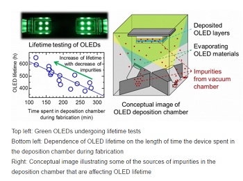
Reproducibility is a necessity for science but has often eluded researchers studying the lifetime of organic light-emitting diodes (OLEDs). Recent research from Japan sheds new light on why: impurities present in the vacuum chamber during fabrication but in amounts so small that they are easily overlooked.
Organic light-emitting diodes use a stack of organic layers to convert electricity into light, and these organic layers are most commonly fabricated by heating source materials in vacuum to evaporate and deposit them onto a lower temperature substrate.
While issues affecting the efficiency of OLEDs are already well understood, a complete picture of exactly how and why OLEDs degrade and lose brightness over time is still missing.
Complicating matters is that devices fabricated with seemingly the same procedures and conditions but by different research groups often degrade at vastly different rates even when the initial performance is the same.
Unable to attribute these reproducibility issues to known sources such as the amount of residual water in the chamber and the purity of the starting materials, a report published online in Scientific Reports ("Influence of vacuum chamber impurities on the lifetime of organic light-emitting diodes"), adds a new piece to the puzzle by focusing on the analysis of the environment in the vacuum chamber.
"Although we often idealize vacuums as being clean environments, we detected many impurities floating in the vacuum even when the deposition chamber is at room temperature," says lead author Hiroshi Fujimoto, chief researcher at Fukuoka i3-Center for Organic Photonics and Electronics Research (i3-OPERA) and visiting associate professor of Kyushu University.
Because of these impurities in the deposition chamber, the researchers found that the time until an OLED under operation dims by a given amount because of degradation, known as the lifetime, sharply increased for OLEDs that spent a shorter time in the deposition chamber during fabrication.
This trend remained even after considering changes in residual water and source material purity, indicating the importance of controlling and minimizing the device fabrication time, a rarely discussed parameter.
Research partners at Sumika Chemical Analysis Service Ltd. (SCAS) confirmed an increase of accumulated impurities with time by analyzing the materials that deposited on extremely clean silicon wafers that were stored in the deposition chamber when OLED materials were not being evaporated.
Using a technique called liquid chromatography-mass spectrometry, the researchers found that many of the impurities could be traced to previously deposited materials and plasticizers from the vacuum chamber components.
"Really small amounts of these impurities get incorporated into the fabricated devices and are causing large changes in the lifetime," says Professor Chihaya Adachi, director of Kyushu University's Center for Organic Photonics and Electronics Research (OPERA), which also took part in the study.
In fact, the new results suggest that the impurities amount to less than even a single molecular layer.
To improve lifetime reproducibility, a practice often adopted in industry is the use of dedicated deposition chambers for specific materials, but this can be difficult in academic labs, where often only a limited number of deposition systems are available for testing a wide variety of new materials.
In these cases, deposition chamber design and cleaning in addition to control of the deposition time are especially important.
"This is an excellent reminder of just how careful we need to be to do good, reproducible science," comments Professor Adachi.


