


 The Marketing Minute: Cracking the Code of Technical Marketing
 Trouble in Your Tank: Implementing Direct Metallization in Advanced Substrate Packaging


Germanium's Semiconducting and Optical Properties Probed Under Pressure
January 4, 2017 | Carnegie Institution for ScienceEstimated reading time: 2 minutes
Germanium may not be a household name like silicon, its group-mate on the periodic table, but it has great potential for use in next-generation electronics and energy technology.
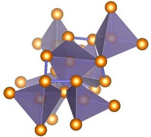
This is an illustration of ST12-germanium's complex tetragonal structure with tetrahedral bonding. (Image: Haidong Zhang)
Of particular interest are forms of germanium that can be synthesized in the lab under extreme pressure conditions. However, one of the most-promising forms of germanium for practical applications, called ST12, has only been created in tiny sample sizes--too small to definitively confirm its properties.
"Attempts to experimentally or theoretically pin down ST12-germanium's characteristics produced extremely varied results, especially in terms of its electrical conductivity," said Carnegie's Zhisheng Zhao, the first author on a new paper about this form of germanium.
The study's research team, led by Carnegie's Timothy Strobel, was able to create ST12-germanium in a large enough sample size to confirm its characteristics and useful properties. Their work is published by Nature Communications ("Properties of the exotic metastable ST12 germanium allotrope").
"This work will be of interest to a broad range of readers in the field of materials science, physics, chemistry, and engineering," explained Carnegie's Haidong Zhang, the co-leading author.
ST12-germanium has a tetragonal structure--the nameST12 means "simple tetragonal with 12 atoms." It was created by putting germanium under about 138 times normal atmospheric pressure (14 gigapascals) and then decompressing it slowly at room temperature.
The millimeter-sized samples of ST12-germanium that the team created were large enough that they could be studied using a variety of spectroscopic techniques in order to confirm its long-debated characteristics.
Like the most common, diamond-cubic form of germanium, they found that ST12 is a semiconductor with a so-called indirect band gap. Metallic substances conduct electrical current easily, whereas insulating materials conduct no current at all. Semiconducting materials exhibit mid-range electrical conductivity. When semiconducting materials are subjected to an input of a specific energy, bound electrons can be moved to higher-energy, conducting states. The specific energy required to make this jump to the conducting state is defined as the "band gap." While direct band gap materials can effectively absorb and emit light, indirect band gap materials cannot.
"Our team was able to quantify ST12's optical band gap--where visible light energy can be absorbed by the material--as well as its electrical and thermal properties, which will help define its potential for practical applications," Strobel said. "Our findings indicate that due to the size of its band gap, ST12-germanium may be a better material for infrared detection and imaging technology than the diamond-cubic form of the element already being used for these purposes."
Share on:


Testimonial
"In a year when every marketing dollar mattered, I chose to keep I-Connect007 in our 2025 plan. Their commitment to high-quality, insightful content aligns with Koh Young’s values and helps readers navigate a changing industry. "
Brent Fischthal - Koh YoungSuggested Items
Curing and Verification in PCB Shadow Areas
09/17/2025 | Doug Katze, DymaxDesign engineers know a simple truth that often complicates electronics manufacturing: Light doesn’t go around corners. In densely populated PCBs, adhesives and coatings often fail to fully cure in shadowed regions created by tall ICs, connectors, relays, and tight housings.
Marcy’s Musings: Advancing the Advanced Materials Discussion
09/17/2025 | Marcy LaRont -- Column: Marcy's MusingsAs the industry’s most trusted global source of original content about the electronics supply chain, we continually ask you about your concerns, what you care about, and what you most want to learn about. Your responses are insightful and valuable. Thank you for caring enough to provide useful feedback and engage in dialogue.
September 2025 PCB007 Magazine: The Future of Advanced Materials
09/16/2025 | I-Connect007 Editorial TeamMoore’s Law is no more, and the advanced material solutions being developed to grapple with this reality are surprising, stunning, and perhaps a bit daunting. Buckle up for a dive into advanced materials and a glimpse into the next chapters of electronics manufacturing.
I-Connect007 Launches Advanced Electronics Packaging Digest
09/15/2025 | I-Connect007I-Connect007 is pleased to announce the launch of Advanced Electronics Packaging Digest (AEPD), a new monthly digital newsletter dedicated to one of the most critical and rapidly evolving areas of electronics manufacturing: advanced packaging at the interconnect level.
Panasonic Industry will Double the Production Capacity of MEGTRON Multi-layer Circuit Board Materials Over the Next Five Years
09/15/2025 | Panasonic Industry Co., Ltd.Panasonic Industry Co., Ltd., a Panasonic Group company, announced plans for a major expansion of its global production capacity for MEGTRON multi-layer circuit board materials today. The company plans to double its production over the next five years to meet growing demand in the AI server and ICT infrastructure markets.