


 Dan's Biz Bookshelf: 'Getting Naked: A Business Fable'
 The Chemical Connection: Common Misconceptions in Wet Processing
 It’s Only Common Sense: Selling to Engineers


Silver Nanowire Inks Enable Paper-based Printable Electronics
January 4, 2017 | Duke UniversityEstimated reading time: 3 minutes
By suspending tiny metal nanoparticles in liquids, Duke University scientists are brewing up conductive ink-jet printer "inks" to print inexpensive, customizable circuit patterns on just about any surface.
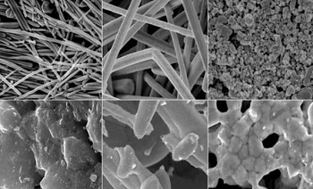
Duke University chemists have found that silver nanowire films like these conduct electricity well enough to form functioning circuits without applying high temperatures, enabling printable electronics on heat-sensitive materials like paper or plastic. (Image: Ian Stewart and Benjamin Wiley)
Printed electronics, which are already being used on a wide scale in devices such as the anti-theft radio frequency identification (RFID) tags you might find on the back of new DVDs, currently have one major drawback: for the circuits to work, they first have to be heated to melt all the nanoparticles together into a single conductive wire, making it impossible to print circuits on inexpensive plastics or paper.
A new study by Duke researchers shows that tweaking the shape of the nanoparticles in the ink might just eliminate the need for heat.
By comparing the conductivity of films made from different shapes of silver nanostructures, the researchers found that electrons zip through films made of silver nanowires much easier than films made from other shapes, like nanospheres or microflakes. In fact, electrons flowed so easily through the nanowire films that they could function in printed circuits without the need to melt them all together.
"The nanowires had a 4,000 times higher conductivity than the more commonly used silver nanoparticles that you would find in printed antennas for RFID tags," said Benjamin Wiley, assistant professor of chemistry at Duke. "So if you use nanowires, then you don't have to heat the printed circuits up to such high temperature and you can use cheaper plastics or paper."
"There is really nothing else I can think of besides these silver nanowires that you can just print and it's simply conductive, without any post-processing," Wiley added.
These types of printed electronics could have applications far beyond smart packaging; researchers envision using the technology to make solar cells, printed displays, LEDS, touchscreens, amplifiers, batteries and even some implantable bio-electronic devices. The results appeared online in ACS Applied Materials and Interfaces ("Effect of Morphology on the Electrical Resistivity of Silver Nanostructure Films").
Silver has become a go-to material for making printed electronics, Wiley said, and a number of studies have recently appeared measuring the conductivity of films with different shapes of silver nanostructures. However, experimental variations make direct comparisons between the shapes difficult, and few reports have linked the conductivity of the films to the total mass of silver used, an important factor when working with a costly material.
"We wanted to eliminate any extra materials from the inks and simply hone in on the amount of silver in the films and the contacts between the nanostructures as the only source of variability," said Ian Stewart, a recent graduate student in Wiley's lab and first author on the ACS paper.
Stewart used known recipes to cook up silver nanostructures with different shapes, including nanoparticles, microflakes, and short and long nanowires, and mixed these nanostructures with distilled water to make simple "inks." He then invented a quick and easy way to make thin films using equipment available in just about any lab -- glass slides and double-sided tape.
"We used a hole punch to cut out wells from double-sided tape and stuck these to glass slides," Stewart said. By adding a precise volume of ink into each tape "well" and then heating the wells -- either to relatively low temperature to simply evaporate the water or to higher temperatures to begin melting the structures together -- he created a variety of films to test.
The team say they weren't surprised that the long nanowire films had the highest conductivity. Electrons usually flow easily through individual nanostructures but get stuck when they have to jump from one structure to the next, Wiley explained, and long nanowires greatly reduce the number of times the electrons have to make this "jump".
But they were surprised at just how drastic the change was. "The resistivity of the long silver nanowire films is several orders of magnitude lower than silver nanoparticles and only 10 times greater than pure silver," Stewart said.
The team is now experimenting with using aerosol jets to print silver nanowire inks in usable circuits. Wiley says they also want to explore whether silver-coated copper nanowires, which are significantly cheaper to produce than pure silver nanowires, will give the same effect.
Share on:


Suggested Items
Elephantech: For a Greener Tomorrow
04/16/2025 | Marcy LaRont, PCB007 MagazineNobuhiko Okamoto is the global sales and marketing manager for Elephantech Inc., a Japanese startup with a vision to make electronics more sustainable. The company is developing a metal inkjet technology that can print directly on the substrate and then give it a copper thickness by plating. In this interview, he discusses this novel technology's environmental advantages, as well as its potential benefits for the PCB manufacturing and semiconductor packaging segments.
Trouble in Your Tank: Organic Addition Agents in Electrolytic Copper Plating
04/15/2025 | Michael Carano -- Column: Trouble in Your TankThere are numerous factors at play in the science of electroplating or, as most often called, electrolytic plating. One critical element is the use of organic addition agents and their role in copper plating. The function and use of these chemical compounds will be explored in more detail.
IDTechEx Highlights Recyclable Materials for PCBs
04/10/2025 | IDTechExConventional printed circuit board (PCB) manufacturing is wasteful, harmful to the environment and energy intensive. This can be mitigated by the implementation of new recyclable materials and technologies, which have the potential to revolutionize electronics manufacturing.
Connect the Dots: Stop Killing Your Yield—The Hidden Cost of Design Oversights
04/03/2025 | Matt Stevenson -- Column: Connect the DotsI’ve been in this industry long enough to recognize red flags in PCB designs. When designers send over PCBs that look great on the computer screen but have hidden flaws, it can lead to manufacturing problems. I have seen this happen too often: manufacturing delays, yield losses, and designers asking, “Why didn’t anyone tell me sooner?” Here’s the thing: Minor design improvements can greatly impact manufacturing yield, and design oversights can lead to expensive bottlenecks. Here’s how to find the hidden flaws in a design and avoid disaster.
Real Time with... IPC APEX EXPO 2025: Tariffs and Supply Chains in U.S. Electronics Manufacturing
04/01/2025 | Real Time with...IPC APEX EXPOChris Mitchell, VP of Global Government Relations for IPC, discusses IPC's concerns about tariffs on copper and their impact on U.S. electronics manufacturing. He emphasizes the complexity of supply chains and the need for policymakers to understand their effects.