


 The Marketing Minute: Cracking the Code of Technical Marketing
 Trouble in Your Tank: Implementing Direct Metallization in Advanced Substrate Packaging


Nano-chimneys Can Cool Circuits
January 5, 2017 | Rice UniversityEstimated reading time: 2 minutes
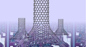
A few nanoscale adjustments may be all that is required to make graphene-nanotube junctions excel at transferring heat, according to Rice University scientists.
The Rice lab of theoretical physicist Boris Yakobson found that putting a cone-like “chimney” between the graphene and nanotube all but eliminates a barrier that blocks heat from escaping.
Heat is transferred through phonons, quasiparticle waves that also transmit sound. The Rice theory offers a strategy to channel damaging heat away from next-generation nano-electronics.
Both graphene and carbon nanotubes consist of six-atom rings, which create a chicken-wire appearance, and both excel at the rapid transfer of electricity and phonons.
But when a nanotube grows from graphene, atoms facilitate the turn by forming heptagonal (seven-member) rings instead. Scientists have determined that forests of nanotubes grown from graphene are excellent for storing hydrogen for energy applications, but in electronics, the heptagons scatter phonons and hinder the escape of heat through the pillars.
The Rice researchers discovered through computer simulations that removing atoms here and there from the two-dimensional graphene base would force a cone to form between the graphene and the nanotube. The geometric properties (aka topology) of the graphene-to-cone and cone-to-nanotube transitions require the same total number of heptagons, but they are more sparsely spaced and leave a clear path of hexagons available for heat to race up the chimney.
“Our interest in advancing new applications for low-dimensional carbon — fullerenes, nanotubes and graphene — is broad,” Yakobson said. “One way is to use them as building blocks to fill three-dimensional spaces with different designs, creating anisotropic, nonuniform scaffolds with properties that none of the current bulk materials have. In this case, we studied a combination of nanotubes and graphene, connected by cones, motivated by seeing such shapes obtained in our colleagues’ experimental labs.”
The researchers tested phonon conduction through simulations of free-standing nanotubes, pillared graphene and nano-chimneys with a cone radius of either 20 or 40 angstroms. The pillared graphene was 20 percent less conductive than plain nanotubes. The 20-angstrom nano-chimneys were just as conductive as plain nanotubes, while 40-angstrom cones were 20 percent better than the nanotubes.
“The tunability of such structures is virtually limitless, stemming from the vast combinatorial possibilities of arranging the elementary modules,” said Alex Kutana, a Rice research scientist and co-author of the study. “The actual challenge is to find the most useful structures given a vast number of possibilities and then make them in the lab reliably.
“In the present case, the fine-tuning parameters could be cone shapes and radii, nanotube spacing, lengths and diameters. Interestingly, the nano-chimneys also act like thermal diodes, with heat flowing faster in one direction than the other,” he said.
Rice graduate student Ziang Zhang is lead author of the paper. Ajit Roy, a principal materials research engineer at the Air Force Research Laboratory in Dayton, Ohio, is a co-author. Yakobson is the Karl F. Hasselmann Professor of Materials Science and NanoEngineering and a professor of chemistry.
Share on:


Testimonial
"Our marketing partnership with I-Connect007 is already delivering. Just a day after our press release went live, we received a direct inquiry about our updated products!"
Rachael Temple - AlltematedSuggested Items
Curing and Verification in PCB Shadow Areas
09/17/2025 | Doug Katze, DymaxDesign engineers know a simple truth that often complicates electronics manufacturing: Light doesn’t go around corners. In densely populated PCBs, adhesives and coatings often fail to fully cure in shadowed regions created by tall ICs, connectors, relays, and tight housings.
Marcy’s Musings: Advancing the Advanced Materials Discussion
09/17/2025 | Marcy LaRont -- Column: Marcy's MusingsAs the industry’s most trusted global source of original content about the electronics supply chain, we continually ask you about your concerns, what you care about, and what you most want to learn about. Your responses are insightful and valuable. Thank you for caring enough to provide useful feedback and engage in dialogue.
September 2025 PCB007 Magazine: The Future of Advanced Materials
09/16/2025 | I-Connect007 Editorial TeamMoore’s Law is no more, and the advanced material solutions being developed to grapple with this reality are surprising, stunning, and perhaps a bit daunting. Buckle up for a dive into advanced materials and a glimpse into the next chapters of electronics manufacturing.
I-Connect007 Launches Advanced Electronics Packaging Digest
09/15/2025 | I-Connect007I-Connect007 is pleased to announce the launch of Advanced Electronics Packaging Digest (AEPD), a new monthly digital newsletter dedicated to one of the most critical and rapidly evolving areas of electronics manufacturing: advanced packaging at the interconnect level.
Panasonic Industry will Double the Production Capacity of MEGTRON Multi-layer Circuit Board Materials Over the Next Five Years
09/15/2025 | Panasonic Industry Co., Ltd.Panasonic Industry Co., Ltd., a Panasonic Group company, announced plans for a major expansion of its global production capacity for MEGTRON multi-layer circuit board materials today. The company plans to double its production over the next five years to meet growing demand in the AI server and ICT infrastructure markets.