


 The Marketing Minute: Cracking the Code of Technical Marketing
 Trouble in Your Tank: Implementing Direct Metallization in Advanced Substrate Packaging


The Bond of Two Stars of Chemistry: Graphene and Porphyrin
January 5, 2017 | Plataforma SINCEstimated reading time: 2 minutes
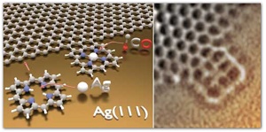
Porphyrins, the same molecules that convey oxygen in haemoglobin and absorb light during photosynthesis, can be joined to the material of the future, graphene, to give it new properties. This was recently shown by a team of scientists at the Technical University of Munich, in which a Spanish researcher also participated (Nature Chemistry, "Fusing tetrapyrroles to graphene edges by surface-assisted covalent coupling"). The resulting hybrid structures could be used in the field of molecular electronics and in developing new sensors.
At the moment, it is difficult to find a material that attracts as much attention from scientists and engineers as graphene, which is made up of a layer of carbon atoms arrange in a hexagonal structure. It is flexible, extremely thin and clear, while being highly resistant and a conductor of electricity – ideal requirements for a number of uses, especially in the field of electronics.
However, using graphene to capture solar energy or as a gas sensor requires specific properties which it lacks, although it can acquire them by addition or functionalisation with certain molecules.
A team of researchers from the Technical University of Munich (TUM), led by Professor Wilhelm Auwärter, has succeeded in bonding an important biochemical group to the graphene sheet: porphyrins, protein rings which are part of chlorophyll, essential for photosynthesis in plants, and haemoglobin, which is responsible for conveying oxygen in animals’ blood.
As Spanish researcher Manuela Garnica Alonso, co-author of the study at the German university, tells SINC, “The new hybrid structures can be used in the field of molecular electronics – in which electronic circuits are composed of molecular units – as well as in catalytic processes in which numerous chemical reactions accelerate, and in the development of new gas sensors.”
The technique involves growing a graphene layer on a surface of silver to use its catalytic properties. Then, under ultra-high vacuum conditions, porphyrin molecules are added. These lose the hydrogen atoms from their periphery when heated on the metal surface, and they end up joining to the graphene edges.
“For the first time we have managed to covalently bond porphyrins to graphene edges, in other words to create stable chemical bonds, without altering their worthwhile properties,” Garnica explains. The researchers used an atomic force microscope to characterise in detail the chemical structure of the molecules involved. With this tool they observed, for example, a metal being incorporated at the centre of the porphyrins, as well as the specific bond of gas molecules, such as carbon dioxide, without altering the graphene properties.
According to the authors, this new graphene ‘functionalisation’ technique could be extended to more molecules in the future, which would bond to various carbon nanostructures, like graphene nanoribbons, while also having great potential in the development of electronic applications.
Share on:


Testimonial
"Advertising in PCB007 Magazine has been a great way to showcase our bare board testers to the right audience. The I-Connect007 team makes the process smooth and professional. We’re proud to be featured in such a trusted publication."
Klaus Koziol - atgSuggested Items
Driving Innovation: Depth Routing Processes—Achieving Unparalleled Precision in Complex PCBs
09/08/2025 | Kurt Palmer -- Column: Driving InnovationIn PCB manufacturing, the demand for increasingly complex and miniaturized designs continually pushes the boundaries of traditional fabrication methods, including depth routing. Success in these applications demands not only on robust machinery but also sophisticated control functions. PCB manufacturers rely on advanced machine features and process methodologies to meet their precise depth routing goals. Here, I’ll explore some crucial functions that empower manufacturers to master complex depth routing challenges.
Polar Instruments Announces Additive Transmission Line Support for Si9000e
08/20/2025 | Polar InstrumentsTransmission lines embedded into the PCB surface are a feature of UHDI constructions. The 2025 fall release of Polar's Si9000e PCB impedance & insertion loss transmission line field solver incorporates eight new single ended, differential and coplanar transmission line structures.
Henniker Plasma Launches Stratus Turnkey Plasma Manufacturing Cell
08/13/2025 | Henniker PlasmaHenniker Plasma, a leading manufacturer of plasma treatment systems, proudly announces the launch of its Stratus Plasma Manufacturing Cell range — a fully integrated, turnkey solution that combines advanced atmospheric plasma surface treatment with robotic automation.
Trouble in Your Tank: Metallizing Flexible Circuit Materials—Mitigating Deposit Stress
08/04/2025 | Michael Carano -- Column: Trouble in Your TankMetallizing materials, such as polyimide used for flexible circuitry and high-reliability multilayer printed wiring boards, provide a significant challenge for process engineers. Conventional electroless copper systems often require pre-treatments with hazardous chemicals or have a small process window to achieve uniform coverage without blistering. It all boils down to enhancing the adhesion of the thin film of electroless copper to these smooth surfaces.
Designers Notebook: Basic PCB Planning Criteria—Establishing Design Constraints
07/22/2025 | Vern Solberg -- Column: Designer's NotebookPrinted circuit board development flows more smoothly when all critical issues are predefined and understood from the start. As a basic planning strategy, the designer must first consider the product performance criteria, then determine the specific industry standards or specifications that the product must meet. Planning also includes a review of all significant issues that may affect the product’s manufacture, performance, reliability, overall quality, and safety.