


 The Marketing Minute: Cracking the Code of Technical Marketing
 Trouble in Your Tank: Implementing Direct Metallization in Advanced Substrate Packaging


NRL Develops Novel Monolayer Ferroelectric Hybrid Structures
January 6, 2017 | NRLEstimated reading time: 3 minutes
Scientists at the U.S. Naval Research Laboratory (NRL), Materials Science and Technology Division, have demonstrated that the intensity and spectral composition of the photoluminescence emitted from a single monolayer of tungsten disulphide (WS2) can be spatially controlled by the polarization domains in an adjacent film of the ferroelectric material lead zirconium titanate (PZT).
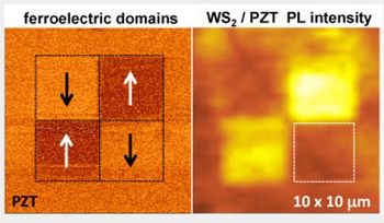
Domains consisting of electric polarization dipoles are written in a checkerboard pattern into a thin film of lead zirconium titanate (PZT) with a conductive atomic force microscope, and imaged with the same instrument (left panel). Both intensity and spectral distribution of the photoluminescence emitted from a monolayer of tungsten disulphide (WS2) transferred onto the PZT surface is strongly modulated by these polarization domains (right panel). (U.S. Naval Research Laboratory)
These domains are written in the PZT using a conductive atomic force microscope, and the photoluminescence (PL) is measured in air at room temperature. Because the polarization domain wall width in a ferroelectric can be as low as 1-10 nm, this approach enables spatial modulation of PL intensity and the corresponding carrier populations with potential for nanoscale resolution.
Single monolayer transition metal dichalcogenides (TMDs) such as WS2 exhibit striking optical properties due to their direct band gap. The dielectric screening is very low due to their two dimensional (2D) character, and thus their properties are strongly affected by their immediate environment, and can be modified and controlled by variations in local charge density due to adsorbates or electrostatic gating. This has generated keen interest in a wide variety of electronic and optical device applications.
The NRL scientist used a conducting atomic force microscope to write polarization domains into a PZT film in a checkerboard pattern. In each domain, the polarization dipole points either up out of the surface plane or down into the surface plane, and produces either positive or negative charge on the PZT surface, respectively. The team then transferred monolayer WS2 that they had grown by chemical vapor deposition techniques onto the PZT film.
They found that the PL intensity from the WS2 is high only from the areas over domains in the PZT where the polarization dipole points out of the surface plane, as shown in the adjacent figure. Further analysis revealed that the spectral composition of the PL was also strongly affected — the spectra from the “up” domains were dominated by neutral exciton contributions (a bound state of an electron and hole arising from Coulomb interaction), while those from the “down” domains were dominated by negatively charged exciton, or trion, contributions (an exciton with an extra electron).
“Fabricating these hybrid 2D/3D ferroelectric heterostructures enables one to purposefully design and modulate adjacent populations of trions and neutral excitons, creating lateral domains in any geometry of choice” notes Dr. Berend Jonker, senior scientist and principal investigator. Dr. Connie Li, lead author of the study, further points out: “Because the FE domains can be rewritten with an atomic force microscope and are non-volatile, this enables spatial modulation of the TMD properties with nanometer scale resolution.”
The payoff includes development of TMD materials and hybrid 2D/3D heterostructures with new functionality relevant to the DoD mission, including ultra-low power electronics, non-volatile optical memory and quantum computation for future DoD applications in information processing and sensing. The research results are reported in the December 4, 2016, issue of ACS Omega (DOI: 10.1021/acsomega.6b00302), the open access journal of the American Chemical Society. The paper was also selected as an ACS Editors’ Choice featured paper. The research team included Dr. Connie Li, Dr. Kathleen McCreary, and Dr. Berend Jonker from the Magnetoelectronic Materials & Devices Section in the Materials Science and Technology Division at NRL.
Share on:


Testimonial
"Our marketing partnership with I-Connect007 is already delivering. Just a day after our press release went live, we received a direct inquiry about our updated products!"
Rachael Temple - AlltematedSuggested Items
Curing and Verification in PCB Shadow Areas
09/17/2025 | Doug Katze, DymaxDesign engineers know a simple truth that often complicates electronics manufacturing: Light doesn’t go around corners. In densely populated PCBs, adhesives and coatings often fail to fully cure in shadowed regions created by tall ICs, connectors, relays, and tight housings.
Marcy’s Musings: Advancing the Advanced Materials Discussion
09/17/2025 | Marcy LaRont -- Column: Marcy's MusingsAs the industry’s most trusted global source of original content about the electronics supply chain, we continually ask you about your concerns, what you care about, and what you most want to learn about. Your responses are insightful and valuable. Thank you for caring enough to provide useful feedback and engage in dialogue.
September 2025 PCB007 Magazine: The Future of Advanced Materials
09/16/2025 | I-Connect007 Editorial TeamMoore’s Law is no more, and the advanced material solutions being developed to grapple with this reality are surprising, stunning, and perhaps a bit daunting. Buckle up for a dive into advanced materials and a glimpse into the next chapters of electronics manufacturing.
I-Connect007 Launches Advanced Electronics Packaging Digest
09/15/2025 | I-Connect007I-Connect007 is pleased to announce the launch of Advanced Electronics Packaging Digest (AEPD), a new monthly digital newsletter dedicated to one of the most critical and rapidly evolving areas of electronics manufacturing: advanced packaging at the interconnect level.
Panasonic Industry will Double the Production Capacity of MEGTRON Multi-layer Circuit Board Materials Over the Next Five Years
09/15/2025 | Panasonic Industry Co., Ltd.Panasonic Industry Co., Ltd., a Panasonic Group company, announced plans for a major expansion of its global production capacity for MEGTRON multi-layer circuit board materials today. The company plans to double its production over the next five years to meet growing demand in the AI server and ICT infrastructure markets.