


 The Marketing Minute: Cracking the Code of Technical Marketing
 Trouble in Your Tank: Implementing Direct Metallization in Advanced Substrate Packaging


New Technology Creates Images Beyond Visible Spectrum on a Single Chip
January 6, 2017 | Duke UniversityEstimated reading time: 4 minutes
Duke University researchers believe they have overcome a longstanding hurdle to producing cheaper, more robust ways to print and image across a range of colors extending into the infrared.
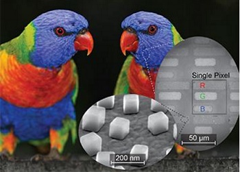
The inlay on this color and infrared image of parrots shows how a simple RGB color scheme was created by building rectangles of varying lengths for each of the colors, as well as individual nanocubes on top of a gold film that create the plasmonic element. Credit - imageBROKER / Alamy Stock Photo
As any mantis shrimp will tell you, there are a wide range of "colors" along the electromagnetic spectrum that humans cannot see but which provide a wealth of information. Sensors that extend into the infrared can, for example, identify thousands of plants and minerals, diagnose cancerous melanomas and predict weather patterns, simply by the spectrum of light they reflect.
Current imaging technologies that can detect infrared wavelengths are expensive and bulky, requiring numerous filters or complex assemblies in front of an infrared photodetector. The need for mechanical movement in such devices reduces their expected lifetime and can be a liability in harsh conditions, such as those experienced by satellites.
In a new paper, a team of Duke engineers reveals a manufacturing technique that promises to bring a simplified form of multispectral imaging into daily use. Because the process uses existing materials and fabrication techniques that are inexpensive and easily scalable, it could revolutionize any industry where multispectral imaging or printing is used.
"It's challenging to create sensors that can detect both the visible spectrum and the infrared," said Maiken Mikkelsen, the Nortel Networks Assistant Professor of Electrical and Computer Engineering and Physics at Duke.
"Traditionally you need different materials that absorb different wavelengths, and that gets very expensive," Mikkelsen said. "But with our technology, the detectors' responses are based on structural properties that we design rather than a material's natural properties. What's really exciting is that we can pair this with a photodetector scheme to combine imaging in both the visible spectrum and the infrared on a single chip."
The new technology relies on plasmonics -- the use of nanoscale physical phenomena to trap certain frequencies of light.
Engineers fashion silver cubes just 100 nanometers wide and place them only a few nanometers above a thin gold foil. When incoming light strikes the surface of a nanocube, it excites the silver's electrons, trapping the light's energy -- but only at a certain frequency.
The size of the silver nanocubes and their distance from the base layer of gold determines that frequency, while controlling the spacing between the nanoparticles allows tuning the strength of the absorption. By precisely tailoring these spacings, researchers can make the system respond to any specific color they want, all the way from visible wavelengths out to the infrared.
A closeup of the colorful parrot picture printed on a thin gold wafer using the new nanocube-based technology. The colors appear off because of the underlying gold, as well as the difficulties that typical cameras have of imaging the new technology.
The challenge facing the engineers is how to build a useful device that could be scalable and inexpensive enough to use in the real world. For that, Mikkelsen turned to her research team, including graduate student Jon Stewart.
"Similar types of materials have been demonstrated before, but they've all used expensive techniques that have kept the technology from transitioning to the market," said Stewart. "We've come up with a fabrication scheme that is scalable, doesn't need a clean room and avoids using million-dollar machines, all while achieving higher frequency sensitivities. It has allowed us to do things in the field that haven't been done before."
To build a detector, Mikkelsen and Stewart used a process of light etching and adhesives to pattern the nanocubes into pixels containing different sizes of silver nanocubes, and thus each sensitive to a specific wavelength of light. When incoming light strikes the array, each area responds differently depending on the wavelength of light it is sensitive to. By teasing out how each part of the array responds, a computer can reconstruct what color the original light was.
The technique can be used for printing as well, the team showed. Instead of creating pixels with six sections tuned to respond to specific colors, they created pixels with three bars that reflect three colors: blue, green and red. By controlling the relative lengths of each bar, they can dictate what combination of colors the pixel reflects. It's a novel take on the classic RGB scheme first used in photography in 1861.
But unlike most other applications, the plasmonic color scheme promises to never fade over time and can be reliably reproduced with tight accuracy time and again. It also allows its adopters to create color schemes in the infrared.
"Again, the exciting part is being able to print in both visible and infrared on the same substrate," said Mikkelsen. "You could imagine printing an image with a hidden portion in the infrared, or even covering an entire object to tailor its spectral response."
Share on:


Testimonial
"The I-Connect007 team is outstanding—kind, responsive, and a true marketing partner. Their design team created fresh, eye-catching ads, and their editorial support polished our content to let our brand shine. Thank you all! "
Sweeney Ng - CEE PCBSuggested Items
Curing and Verification in PCB Shadow Areas
09/17/2025 | Doug Katze, DymaxDesign engineers know a simple truth that often complicates electronics manufacturing: Light doesn’t go around corners. In densely populated PCBs, adhesives and coatings often fail to fully cure in shadowed regions created by tall ICs, connectors, relays, and tight housings.
Marcy’s Musings: Advancing the Advanced Materials Discussion
09/17/2025 | Marcy LaRont -- Column: Marcy's MusingsAs the industry’s most trusted global source of original content about the electronics supply chain, we continually ask you about your concerns, what you care about, and what you most want to learn about. Your responses are insightful and valuable. Thank you for caring enough to provide useful feedback and engage in dialogue.
September 2025 PCB007 Magazine: The Future of Advanced Materials
09/16/2025 | I-Connect007 Editorial TeamMoore’s Law is no more, and the advanced material solutions being developed to grapple with this reality are surprising, stunning, and perhaps a bit daunting. Buckle up for a dive into advanced materials and a glimpse into the next chapters of electronics manufacturing.
I-Connect007 Launches Advanced Electronics Packaging Digest
09/15/2025 | I-Connect007I-Connect007 is pleased to announce the launch of Advanced Electronics Packaging Digest (AEPD), a new monthly digital newsletter dedicated to one of the most critical and rapidly evolving areas of electronics manufacturing: advanced packaging at the interconnect level.
Panasonic Industry will Double the Production Capacity of MEGTRON Multi-layer Circuit Board Materials Over the Next Five Years
09/15/2025 | Panasonic Industry Co., Ltd.Panasonic Industry Co., Ltd., a Panasonic Group company, announced plans for a major expansion of its global production capacity for MEGTRON multi-layer circuit board materials today. The company plans to double its production over the next five years to meet growing demand in the AI server and ICT infrastructure markets.