


 The Marketing Minute: Cracking the Code of Technical Marketing
 Trouble in Your Tank: Implementing Direct Metallization in Advanced Substrate Packaging


Researchers Design One of the Strongest, Lightest Materials Known
January 9, 2017 | MITEstimated reading time: 5 minutes
A team of researchers at MIT has designed one of the strongest lightweight materials known, by compressing and fusing flakes of graphene, a two-dimensional form of carbon. The new material, a sponge-like configuration with a density of just 5 percent, can have a strength 10 times that of steel.
In its two-dimensional form, graphene is thought to be the strongest of all known materials. But researchers until now have had a hard time translating that two-dimensional strength into useful three-dimensional materials.
The new findings show that the crucial aspect of the new 3-D forms has more to do with their unusual geometrical configuration than with the material itself, which suggests that similar strong, lightweight materials could be made from a variety of materials by creating similar geometric features.
The findings are being reported today in the journal Science Advances, in a paper by Markus Buehler, the head of MIT’s Department of Civil and Environmental Engineering (CEE) and the McAfee Professor of Engineering; Zhao Qin, a CEE research scientist; Gang Seob Jung, a graduate student; and Min Jeong Kang MEng ’16, a recent graduate.
A team of MIT engineers has successfully designed a new 3-D material with five percent the density of steel and ten times the strength, making it one of the strongest, lightweight materials known. Video: Melanie Gonick/MIT
Other groups had suggested the possibility of such lightweight structures, but lab experiments so far had failed to match predictions, with some results exhibiting several orders of magnitude less strength than expected. The MIT team decided to solve the mystery by analyzing the material’s behavior down to the level of individual atoms within the structure. They were able to produce a mathematical framework that very closely matches experimental observations.
Two-dimensional materials — basically flat sheets that are just one atom in thickness but can be indefinitely large in the other dimensions — have exceptional strength as well as unique electrical properties. But because of their extraordinary thinness, “they are not very useful for making 3-D materials that could be used in vehicles, buildings, or devices,” Buehler says. “What we’ve done is to realize the wish of translating these 2-D materials into three-dimensional structures.”
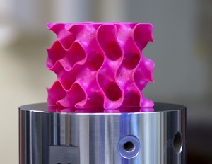
The team was able to compress small flakes of graphene using a combination of heat and pressure. This process produced a strong, stable structure whose form resembles that of some corals and microscopic creatures called diatoms. These shapes, which have an enormous surface area in proportion to their volume, proved to be remarkably strong. “Once we created these 3-D structures, we wanted to see what’s the limit — what’s the strongest possible material we can produce,” says Qin. To do that, they created a variety of 3-D models and then subjected them to various tests. In computational simulations, which mimic the loading conditions in the tensile and compression tests performed in a tensile loading machine, “one of our samples has 5 percent the density of steel, but 10 times the strength,” Qin says.
Buehler says that what happens to their 3-D graphene material, which is composed of curved surfaces under deformation, resembles what would happen with sheets of paper. Paper has little strength along its length and width, and can be easily crumpled up. But when made into certain shapes, for example rolled into a tube, suddenly the strength along the length of the tube is much greater and can support substantial weight. Similarly, the geometric arrangement of the graphene flakes after treatment naturally forms a very strong configuration.
The new configurations have been made in the lab using a high-resolution, multimaterial 3-D printer. They were mechanically tested for their tensile and compressive properties, and their mechanical response under loading was simulated using the team’s theoretical models. The results from the experiments and simulations matched accurately.
The new, more accurate results, based on atomistic computational modeling by the MIT team, ruled out a possibility proposed previously by other teams: that it might be possible to make 3-D graphene structures so lightweight that they would actually be lighter than air, and could be used as a durable replacement for helium in balloons. The current work shows, however, that at such low densities, the material would not have sufficient strength and would collapse from the surrounding air pressure.
But many other possible applications of the material could eventually be feasible, the researchers say, for uses that require a combination of extreme strength and light weight. “You could either use the real graphene material or use the geometry we discovered with other materials, like polymers or metals,” Buehler says, to gain similar advantages of strength combined with advantages in cost, processing methods, or other material properties (such as transparency or electrical conductivity).
“You can replace the material itself with anything,” Buehler says. “The geometry is the dominant factor. It’s something that has the potential to transfer to many things.”
The unusual geometric shapes that graphene naturally forms under heat and pressure look something like a Nerf ball — round, but full of holes. These shapes, known as gyroids, are so complex that “actually making them using conventional manufacturing methods is probably impossible,” Buehler says. The team used 3-D-printed models of the structure, enlarged to thousands of times their natural size, for testing purposes.
For actual synthesis, the researchers say, one possibility is to use the polymer or metal particles as templates, coat them with graphene by chemical vapor deposit before heat and pressure treatments, and then chemically or physically remove the polymer or metal phases to leave 3-D graphene in the gyroid form. For this, the computational model given in the current study provides a guideline to evaluate the mechanical quality of the synthesis output.
The same geometry could even be applied to large-scale structural materials, they suggest. For example, concrete for a structure such a bridge might be made with this porous geometry, providing comparable strength with a fraction of the weight. This approach would have the additional benefit of providing good insulation because of the large amount of enclosed airspace within it.
Because the shape is riddled with very tiny pore spaces, the material might also find application in some filtration systems, for either water or chemical processing. The mathematical descriptions derived by this group could facilitate the development of a variety of applications, the researchers say.
“This is an inspiring study on the mechanics of 3-D graphene assembly,” says Huajian Gao, a professor of engineering at Brown University, who was not involved in this work. “The combination of computational modeling with 3-D-printing-based experiments used in this paper is a powerful new approach in engineering research. It is impressive to see the scaling laws initially derived from nanoscale simulations resurface in macroscale experiments under the help of 3-D printing,” he says.
This work, Gao says, “shows a promising direction of bringing the strength of 2-D materials and the power of material architecture design together.”
The research was supported by the Office of Naval Research, the Department of Defense Multidisciplinary University Research Initiative, and BASF-North American Center for Research on Advanced Materials.
Share on:


Testimonial
"The I-Connect007 team is outstanding—kind, responsive, and a true marketing partner. Their design team created fresh, eye-catching ads, and their editorial support polished our content to let our brand shine. Thank you all! "
Sweeney Ng - CEE PCBSuggested Items
Curing and Verification in PCB Shadow Areas
09/17/2025 | Doug Katze, DymaxDesign engineers know a simple truth that often complicates electronics manufacturing: Light doesn’t go around corners. In densely populated PCBs, adhesives and coatings often fail to fully cure in shadowed regions created by tall ICs, connectors, relays, and tight housings.
Marcy’s Musings: Advancing the Advanced Materials Discussion
09/17/2025 | Marcy LaRont -- Column: Marcy's MusingsAs the industry’s most trusted global source of original content about the electronics supply chain, we continually ask you about your concerns, what you care about, and what you most want to learn about. Your responses are insightful and valuable. Thank you for caring enough to provide useful feedback and engage in dialogue.
September 2025 PCB007 Magazine: The Future of Advanced Materials
09/16/2025 | I-Connect007 Editorial TeamMoore’s Law is no more, and the advanced material solutions being developed to grapple with this reality are surprising, stunning, and perhaps a bit daunting. Buckle up for a dive into advanced materials and a glimpse into the next chapters of electronics manufacturing.
I-Connect007 Launches Advanced Electronics Packaging Digest
09/15/2025 | I-Connect007I-Connect007 is pleased to announce the launch of Advanced Electronics Packaging Digest (AEPD), a new monthly digital newsletter dedicated to one of the most critical and rapidly evolving areas of electronics manufacturing: advanced packaging at the interconnect level.
Panasonic Industry will Double the Production Capacity of MEGTRON Multi-layer Circuit Board Materials Over the Next Five Years
09/15/2025 | Panasonic Industry Co., Ltd.Panasonic Industry Co., Ltd., a Panasonic Group company, announced plans for a major expansion of its global production capacity for MEGTRON multi-layer circuit board materials today. The company plans to double its production over the next five years to meet growing demand in the AI server and ICT infrastructure markets.