


 The Marketing Minute: Cracking the Code of Technical Marketing
 Trouble in Your Tank: Implementing Direct Metallization in Advanced Substrate Packaging


NRL Detects Opposite Spin in Topological Insulator Surface States
January 9, 2017 | NRLEstimated reading time: 3 minutes
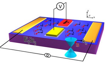
Scientists at the U.S. Naval Research Laboratory (NRL) have reported the first direct comparison of the spin polarization generated in the topologically protected Dirac states of a topological insulator (TI) bismuth selenide (Bi2Se3) and the trivial 2-dimensional electron gas (2DEG) states at the surface of indium arsenide (InAs).
The NRL research team selected the two materials to clearly distinguish the polarization contributions from the linear Dirac and parabolic 2DEG surface states. Identical device structures and measurements were performed on each: Bi2Se3, a topological insulator known to have both linear Dirac and trivial 2DEG surface states; and InAs, a common semiconductor that exhibits only the trivial 2DEG surface states.
To clearly distinguish the polarization contributions from the linear Dirac and parabolic 2DEG surface states, the NRL research team selected two materials: Bi2Se3, a topological insulator known to have both linear Dirac and trivial 2DEG surface states; and InAs, a common semiconductor that exhibits only the trivial 2DEG surface states. Identical device structures and measurements were performed on each, as illustrated in the above figure. The spin polarization created by an unpolarized bias current is directly detected as a voltage (V) on a magnetic tunnel barrier contact. (U.S. Naval Research Laboratory)
In each case, the spin polarization is spontaneously generated by an unpolarized bias current, and detected using ferromagnetic metal contacts with an oxide tunnel barrier. The researchers demonstrated that the sign of the spin polarization from these two contributions is opposite, confirming theoretical predictions and establishing InAs as a common reference sample for future experiments.
The team also developed a detailed model based on spin-dependent electrochemical potentials to explicitly derive the sign of the spin voltage expected for the TI surface states, which corroborates their experimental observations and previous theory predictions.
“Detecting this spin polarization directly as a voltage, and differentiating the contributions from these two fundamentally different systems, is key to understanding the basic properties of TI materials and interfacing them to electronic circuitry for future device applications” notes Dr. Connie Li, lead author of the study. Dr. Berend Jonker, senior scientist and principal investigator, points out “The coexistence of these 2DEG states in TI systems has generated considerable controversy in the sign of spin voltage measured. InAs provides a widely available, simply prepared reference sample which research groups around the world may use to benchmark similar polarization measurements in the future.”
Topological insulators constitute a new quantum phase of matter where the bulk is nominally an insulator, but the surface layer is occupied by linearly dispersing metallic states populated by massless Dirac fermions that are topologically protected from perturbations to their environment. The existence of this class of material was predicted from the study of “topology,” a branch of mathematics that describes properties that only change step-wise. The 2016 Nobel Prize in Physics was awarded to three physicists for utilizing topological concepts to study exotic phases of matter which manifest novel quantum properties that may improve future electronics, superconductors, and lead to quantum computers.
One of the most striking properties of topological insulators is that of spin-momentum locking — the spin of an electron in the TI Dirac surface state is locked at right angle to its momentum. This consequently implies that when an unpolarized charge current flows in the topologically protected surface states, a net electron spin polarization should spontaneously appear.
Electrically accessing these states is sometimes complicated by potential band bending at the TI surface that may lead to charge accumulation and formation of trivial 2DEG states with parabolic energy dispersion. These 2DEG states nest within and coexist with the linear Dirac states, and may also generate a spin polarization due to strong Rashba spin-orbit coupling — a momentum-dependent splitting of spin bands in two-dimensional condensed matter systems. Their helical spin texture, or sign of the induced polarization, however, is predicted to be opposite to that of the TI Dirac states, and with smaller magnitude.
The team’s discovery is an essential step in the electrical manipulation of spins in next generation TI and spin-orbit coupling based quantum devices. The research team included Dr. Connie Li, Dr. Olaf van ‘t Erve, and Dr. Berend Jonker from the Magnetoelectronic Materials & Devices Section in the Materials Science and Technology Division at NRL, in collaboration with Prof. Lian Li’s group at the West Virginia University.
Share on:


Testimonial
"Advertising in PCB007 Magazine has been a great way to showcase our bare board testers to the right audience. The I-Connect007 team makes the process smooth and professional. We’re proud to be featured in such a trusted publication."
Klaus Koziol - atgSuggested Items
Curing and Verification in PCB Shadow Areas
09/17/2025 | Doug Katze, DymaxDesign engineers know a simple truth that often complicates electronics manufacturing: Light doesn’t go around corners. In densely populated PCBs, adhesives and coatings often fail to fully cure in shadowed regions created by tall ICs, connectors, relays, and tight housings.
Marcy’s Musings: Advancing the Advanced Materials Discussion
09/17/2025 | Marcy LaRont -- Column: Marcy's MusingsAs the industry’s most trusted global source of original content about the electronics supply chain, we continually ask you about your concerns, what you care about, and what you most want to learn about. Your responses are insightful and valuable. Thank you for caring enough to provide useful feedback and engage in dialogue.
September 2025 PCB007 Magazine: The Future of Advanced Materials
09/16/2025 | I-Connect007 Editorial TeamMoore’s Law is no more, and the advanced material solutions being developed to grapple with this reality are surprising, stunning, and perhaps a bit daunting. Buckle up for a dive into advanced materials and a glimpse into the next chapters of electronics manufacturing.
I-Connect007 Launches Advanced Electronics Packaging Digest
09/15/2025 | I-Connect007I-Connect007 is pleased to announce the launch of Advanced Electronics Packaging Digest (AEPD), a new monthly digital newsletter dedicated to one of the most critical and rapidly evolving areas of electronics manufacturing: advanced packaging at the interconnect level.
Panasonic Industry will Double the Production Capacity of MEGTRON Multi-layer Circuit Board Materials Over the Next Five Years
09/15/2025 | Panasonic Industry Co., Ltd.Panasonic Industry Co., Ltd., a Panasonic Group company, announced plans for a major expansion of its global production capacity for MEGTRON multi-layer circuit board materials today. The company plans to double its production over the next five years to meet growing demand in the AI server and ICT infrastructure markets.