


 The Marketing Minute: Cracking the Code of Technical Marketing
 Trouble in Your Tank: Implementing Direct Metallization in Advanced Substrate Packaging


Lining Up for New High-density Memory Devices
January 10, 2017 | Department of Energy, Office of ScienceEstimated reading time: 2 minutes
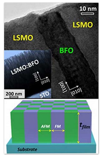
To reduce the size and increase the durability of computers, cell phones, and other data-storing devices, scientists designed a structure made of tiny layers, which resembles a thick chessboard butcher-block table (Nanoscale, "Strong perpendicular exchange bias in epitaxial La0.7Sr0.3MnO3:BiFeO3 nanocomposite films through vertical interfacial coupling").
(Top) Cross-sectional transmission electron microscopy (TEM) image of vertically aligned La0.7Sr0.3MnO3 (LSMO) film showing a BiFeO3 (BFO) pillar embedded in the LSMO matrix. These structures were grown lattice matched onto a SrTiO3 (STO) substrate. The inset shows a low magnification cross-sectional TEM image, illustrating the alternating growth of LSMO and BFO vertical pillars. (Bottom) Schematic illustration of the antiferromagnetic (AFM) and ferromagnetic (FM) layers in the vertically aligned nanocomposite film. In the figure, t = thickness. (Image: Department of Materials Science & Engineering, Texas A&M University)
Using the material, where each layer is made of one of two composites, scientists can vertically manipulate the magnetization, enabling a type of magnetic coupling between two layers commonly employed in magnetic devices. They can “pin,” or set, the magnetic states of the materials at their unique states of maximum sensitivity; this setting is essential for magnetic device stability.
Extremely thin layers of a unique material could lead to the design of new read heads for hard drives and other high-density memory devices that have greater stability when exposed to high temperatures and a smaller size.
Scientists grew a vertically aligned nanocomposites lattice matched on a SrTiO3 (STO) substrate using laser deposition. These micrometer-thick layers exhibited strong, perpendicular (vertical) magnetic coupling (exchange bias).
The degree of structural strain in the nanocomposites effects the magnetic exchange bias behavior (that is, a type of magnetic coupling between two layers commonly employed in magnetic devices).
In addition, the composition of the different layers in the film (La0.7Sr0.3MnO3 [LSMO] and BiFeO3 [BFO]) determines the density, degree of strain accommodation, and magnetic phase transition, which all affect the overall magnetic exchange bias coupling strength.
By controlling the composition of the layers in the nanocomposites, scientists can tune the degree of magnetic exchange bias coupling strength. The research team conducted a microstructural analysis of the nanocomposite films using transmission electron microscopy and scanning transmission electron microscopy. The images show vertical structures with boundaries. They measured the magnetization of the nanocomposites using a magnetometer.
This new nanoscale architecture can be used for data storage in high-density memory devices as an alternative to conventional, in-plane magnetic exchange bias; such devices could provide more efficient performance.
Share on:


Testimonial
"Our marketing partnership with I-Connect007 is already delivering. Just a day after our press release went live, we received a direct inquiry about our updated products!"
Rachael Temple - AlltematedSuggested Items
Knocking Down the Bone Pile: Best Practices for Electronic Component Salvaging
09/17/2025 | Nash Bell -- Column: Knocking Down the Bone PileElectronic component salvaging is the practice of recovering high-value devices from PCBs taken from obsolete or superseded electronic products. These components can be reused in new assemblies, reducing dependence on newly purchased parts that may be costly or subject to long lead times.
Global Interposer Market to Surge Nearly Fivefold by 2034
09/15/2025 | I-Connect007 Editorial TeamRevenue for the global interposer market is projected to climb from $471 million in 2025 to more than $2.3 billion by 2034, according to a new report from Business Research Insights. The growth represents a CAGR of nearly 20 percent over the forecast period.
AI-Powered Wearables Transform How Consumers Interact with Everyday Technology
09/15/2025 | PR NewswireThe global demand for AI-driven, touchless wearable technologies is accelerating as consumers seek more natural, seamless and intuitive ways to interact with their devices. Traditional touch screens and voice assistants, while effective, are increasingly viewed as limiting in a world where multitasking, mobility and efficiency are key. As industries from consumer electronics to augmented reality and enterprise computing embrace the possibilities of gesture-based control, the market for neural interfaces is rapidly expanding
ROHM Develops Ultra-Compact CMOS Op Amp: Delivering Industry-Leading Ultra-Low Circuit Current
09/11/2025 | ROHMROHM’s ultra-compact CMOS Operational Amplifier (op amp) TLR1901GXZ achieves the industry’s lowest operating circuit current.
Medical Device Contract Manufacturing Market Worth $140.84 Billion by 2030 with 10.9% CAGR
08/25/2025 | PRNewswireThe global Medical Device Contract Manufacturing Market, valued at US$78.58 billion in 2024, stood at US$83.77 billion in 2025 and is projected to advance at a resilient CAGR of 10.9% from 2025 to 2030, culminating in a forecasted valuation of US$140.84 billion by the end of the period.