


 The Marketing Minute: Cracking the Code of Technical Marketing
 Trouble in Your Tank: Implementing Direct Metallization in Advanced Substrate Packaging


A Modular Valve Simplifies Diagnostic Chip Fabrication
January 11, 2017 | A*STAREstimated reading time: 2 minutes
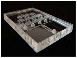
Swapping delicate microscopic flow valves for a universal modular valve system has enabled A*STAR researchers to dramatically decrease the cost and complexity of microfluidic diagnostic chips — business card-sized devices that can analyse blood on the spot for a range of disease biomarkers (Microfluidics and Nanofluidics, "Modular membrane valves for universal integration within thermoplastic devices").
A microfluidic device made by A*STAR scientists for on-the-spot blood analysis. (Image: A*STAR Singapore Institute of Manufacturing Technology)
“Microfluidic chips are advancing point-of-care diagnosis for many diseases,” says Alicia Toh from A*STAR’s Singapore Institute of Manufacturing Technology (SIMTech). “Inside these chips, tiny microvalves precisely direct microlitres of fluid through a series of microchannels for automated analysis. However, integrating microvalves into the microchannels is complex and highly susceptible to fabrication defects, which translates into a higher cost per device. In the medical diagnostic sector the race is on to lower the cost per diagnosis by producing cheaper microfluidic diagnostic chips.”
Toh and her colleagues Zhiping Wang and Zhenfeng Wang addressed the problem by moving the microvalves off the main microfluidic chip, and created a modular valve that is fitted to the surface of the chip after fabrication. The valves consist of a microfluidic channel that connects to surface ports on the chip, and an air chamber that allows the channel to be pinched by increasing the air pressure. The team demonstrated that their modular valves could precisely manipulate chemical concentrations through fluidic routing, which is critical in many advance diagnostic applications.
“By mass producing these microvalve modules separate from the microfluidic chip and testing valve function prior to chip integration, we can achieve much lower defect rates, which boosts yields and results in a much lower cost per device,” says Toh. “This technology will reduce waste and help contribute to sustainable manufacturing practices for microfluidic chips.”
Getting the valve design right, however, was complicated. The team used state-of-the-art software to predict the microscopic interactions between the flexible elastomeric silicone membrane and the fluid in the microchannel. Using materials that are compatible with the latest microfluidics technologies was also a big constraint.
“The industry is rapidly moving toward more cost effective thermoplastic materials,” says Toh. “By using compatible materials, we can achieve reliable integration without additional surface modification or adhesives.”
Toh and her team are now exploring the production of microvalve modules using a variety of novel materials. “Greater adoption of microfluidic technology will mean that we could see our modular microvalves being used in a wide spectrum of applications,” she says.
Share on:


Testimonial
"Advertising in PCB007 Magazine has been a great way to showcase our bare board testers to the right audience. The I-Connect007 team makes the process smooth and professional. We’re proud to be featured in such a trusted publication."
Klaus Koziol - atgSuggested Items
Curing and Verification in PCB Shadow Areas
09/17/2025 | Doug Katze, DymaxDesign engineers know a simple truth that often complicates electronics manufacturing: Light doesn’t go around corners. In densely populated PCBs, adhesives and coatings often fail to fully cure in shadowed regions created by tall ICs, connectors, relays, and tight housings.
Marcy’s Musings: Advancing the Advanced Materials Discussion
09/17/2025 | Marcy LaRont -- Column: Marcy's MusingsAs the industry’s most trusted global source of original content about the electronics supply chain, we continually ask you about your concerns, what you care about, and what you most want to learn about. Your responses are insightful and valuable. Thank you for caring enough to provide useful feedback and engage in dialogue.
September 2025 PCB007 Magazine: The Future of Advanced Materials
09/16/2025 | I-Connect007 Editorial TeamMoore’s Law is no more, and the advanced material solutions being developed to grapple with this reality are surprising, stunning, and perhaps a bit daunting. Buckle up for a dive into advanced materials and a glimpse into the next chapters of electronics manufacturing.
I-Connect007 Launches Advanced Electronics Packaging Digest
09/15/2025 | I-Connect007I-Connect007 is pleased to announce the launch of Advanced Electronics Packaging Digest (AEPD), a new monthly digital newsletter dedicated to one of the most critical and rapidly evolving areas of electronics manufacturing: advanced packaging at the interconnect level.
Panasonic Industry will Double the Production Capacity of MEGTRON Multi-layer Circuit Board Materials Over the Next Five Years
09/15/2025 | Panasonic Industry Co., Ltd.Panasonic Industry Co., Ltd., a Panasonic Group company, announced plans for a major expansion of its global production capacity for MEGTRON multi-layer circuit board materials today. The company plans to double its production over the next five years to meet growing demand in the AI server and ICT infrastructure markets.