


 The Marketing Minute: Cracking the Code of Technical Marketing
 Trouble in Your Tank: Implementing Direct Metallization in Advanced Substrate Packaging


Sketching Out Magnetism with Electricity
January 13, 2017 | SLAC National Accelerator LaboratoryEstimated reading time: 3 minutes
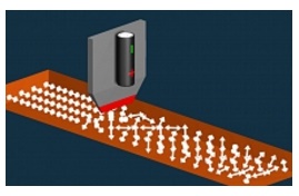
In a proof-of-concept study published in Nature Physics, researchers drew magnetic squares in a nonmagnetic material with an electrified pen and then “read” this magnetic doodle with X-rays.
In the experiment, the scientists moved the electric tip along the surface and applied a positive voltage. The electric field aligns the spins of the electrons in the nonmagnetic material, and the ordering creates magnetic properties. If the voltage is reversed, the spins once again become disordered and magnetism is lost. The researchers were able to see the changes using X-ray microscopy at the Stanford Synchrotron Radiation Lightsource. (SLAC National Accelerator Laboratory)
The experiment demonstrated that magnetic properties can be created and annihilated in a nonmagnetic material with precise application of an electric field – something long sought by scientists looking for a better way to store and retrieve information on hard drives and other magnetic memory devices. The research took place at the Department of Energy’s SLAC National Accelerator Laboratory and the Korea Advanced Institute of Science and Technology.
“The important thing is that it’s reversible. Changing the voltage of the applied electric field demagnetizes the material again,” said Hendrik Ohldag, a co-author on the paper and scientist at the lab’s Stanford Synchrotron Radiation Lightsource (SSRL), a DOE Office of Science User Facility.
“That means this technique could be used to design new types of memory storage devices with additional layers of information that can be turned on and off with an electric field, rather than the magnetic fields used today,” Ohldag said. “This would allow more targeted control, and would be less likely to cause unwanted effects in surrounding magnetic areas.”
“This experimental finding is important for overcoming the current difficulties in storage applications,” said Jun-Sik Lee, a SLAC staff scientist and one of the leaders of the experiment. “We can now make a definitive statement: This approach can be implemented to design future storage devices.”
Lining Up the Spins
A material's magnetic properties are determined by the orientation of the electrons’ spins. In ferromagnetic materials, found in hard drives, refrigerator magnets and compass needles, all the electron spins are lined up in the same direction. These spins can be manipulated by applying a magnetic field – flipping them from north to south, for instance, to store information as ones and zeroes.
Scientists have also been trying different ways to create a “multiferroic state,” where magnetism can be manipulated with an electrical field.
“This has become one of the Holy Grails of technology over the past decade,” Ohldag said. “There are studies that have shown aspects of this multiferroic state before. The novelty here is that by designing a particular material, we managed to both create and eliminate magnetism in a controlled fashion on the nanoscale.”
Crosstalk Between Electricity and Magnetism
In this study, the team started with an antiferromagnetic material – one that has small patches of magnetism that cancel each other out, so that overall it doesn’t act like a magnet.
Both antiferromagnets and ferromagnets show magnetic properties only below a certain temperature, and above that temperature they become non-magnetic.
By designing an antiferromagnetic material doped with the element lanthanum, the researchers found they could tune the properties of the material in such a way that electricity and magnetism could influence each other at room temperature. They could then flip the magnetic properties with an electrical field.
To see these changes, they tuned a scanning transmission X-ray microscope at SSRL so it could detect the magnetic spin of the electrons. The X-ray images confirmed that the magnetization had occurred, and was truly reversible.
Next, the research team would like to test other materials, to see if they can find a way to make the effect even more pronounced.
The research team included scientists from the Korea Institute of Materials Science, Pohang University of Science and Technology, Pohang National Accelerator Laboratory, Max Planck Institute for Chemical Physics of Solids and the University of New South Wales of Australia.
Share on:


Testimonial
"In a year when every marketing dollar mattered, I chose to keep I-Connect007 in our 2025 plan. Their commitment to high-quality, insightful content aligns with Koh Young’s values and helps readers navigate a changing industry. "
Brent Fischthal - Koh YoungSuggested Items
Curing and Verification in PCB Shadow Areas
09/17/2025 | Doug Katze, DymaxDesign engineers know a simple truth that often complicates electronics manufacturing: Light doesn’t go around corners. In densely populated PCBs, adhesives and coatings often fail to fully cure in shadowed regions created by tall ICs, connectors, relays, and tight housings.
Marcy’s Musings: Advancing the Advanced Materials Discussion
09/17/2025 | Marcy LaRont -- Column: Marcy's MusingsAs the industry’s most trusted global source of original content about the electronics supply chain, we continually ask you about your concerns, what you care about, and what you most want to learn about. Your responses are insightful and valuable. Thank you for caring enough to provide useful feedback and engage in dialogue.
September 2025 PCB007 Magazine: The Future of Advanced Materials
09/16/2025 | I-Connect007 Editorial TeamMoore’s Law is no more, and the advanced material solutions being developed to grapple with this reality are surprising, stunning, and perhaps a bit daunting. Buckle up for a dive into advanced materials and a glimpse into the next chapters of electronics manufacturing.
I-Connect007 Launches Advanced Electronics Packaging Digest
09/15/2025 | I-Connect007I-Connect007 is pleased to announce the launch of Advanced Electronics Packaging Digest (AEPD), a new monthly digital newsletter dedicated to one of the most critical and rapidly evolving areas of electronics manufacturing: advanced packaging at the interconnect level.
Panasonic Industry will Double the Production Capacity of MEGTRON Multi-layer Circuit Board Materials Over the Next Five Years
09/15/2025 | Panasonic Industry Co., Ltd.Panasonic Industry Co., Ltd., a Panasonic Group company, announced plans for a major expansion of its global production capacity for MEGTRON multi-layer circuit board materials today. The company plans to double its production over the next five years to meet growing demand in the AI server and ICT infrastructure markets.