


 The Marketing Minute: Cracking the Code of Technical Marketing
 Trouble in Your Tank: Implementing Direct Metallization in Advanced Substrate Packaging


Technique Enables Adaptable 3-D Printing
January 13, 2017 | MITEstimated reading time: 3 minutes
Three-dimensional printing technology makes it possible to rapidly manufacture objects by depositing layer upon layer of polymers in a precisely determined pattern. Once these objects are completed, the polymers that form the material are “dead” — that is, they cannot be extended to form new polymer chains.
MIT chemists have now developed a technique that allows them to print objects and then go back and add new polymers that alter the materials’ chemical composition and mechanical properties. The researchers can also fuse two or more printed objects together to form more complex structures.
“The idea is that you could print a material and subsequently take that material and, using light, morph the material into something else, or grow the material further,” says Jeremiah Johnson, the Firmenich Career Development Associate Professor of Chemistry at MIT.
This technique could greatly expand the complexity of objects that can be created with 3-D printing, says Johnson, the senior author of a paper describing the approach in the Jan. 13 issue of ACS Central Science. The paper’s lead authors are former MIT postdoc Mao Chen and graduate student Yuwei Gu.
Living polymerization
One of the most common techniques used for 3-D printing, also known as additive manufacturing, is stereolithography. By shining light onto a liquid solution of monomers, the building blocks of plastic and other materials, stereolithography devices can form layers of solid polymers until the final shape is completed.
Several years ago, Johnson and his colleagues set out to create adaptable 3-D-printed structures by taking advantage of a technique known as “living polymerization,” which yields materials whose growth can be halted and then restarted later on.
In 2013, the researchers demonstrated that they could use a type of polymerization stimulated by ultraviolet light to add new features to 3-D-printed materials. After printing an object, the researchers used ultraviolet light to break apart the polymers at certain points, creating very reactive molecules called free radicals. These radicals would then bind to new monomers from a solution surrounding the object, incorporating them into the original material.
“The advantage there is you can turn the light on and the chains grow, and you turn the light off and they stop,” Johnson says. “In principle, you can repeat that indefinitely and they can continue growing and growing.”
However, this approach proved to be too damaging to the material and difficult to control, because free radicals are so reactive.
New properties
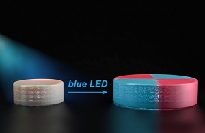
In their next effort, the researchers designed new polymers that are also reactivated by light, but in a slightly different way. Each of the polymers contains chemical groups that act like a folded up accordion. These chemical groups, known as TTCs, can be activated by organic catalysts that are turned on by light. When blue light from an LED shines on the catalyst, it attaches new monomers to the TTCs, making them stretch out. As these monomers are incorporated uniformly throughout the structure, they give the material new properties.
“That’s the breakthrough in this paper: We really have a truly living method where we can take macroscopic materials and grow them in the way we want to,” Johnson says.
In the ACS Central Science paper, the researchers demonstrated that they can incorporate monomers that alter a material’s mechanical properties, such as stiffness, and its chemical properties, including hydrophobicity (affinity for water). They also showed that they could make materials swell and contract in response to temperature by adding a certain type of monomer.
The researchers also used this approach to fuse two structures together, by shining light on the regions where they come in contact with each other.
Cyrille Boyer, an associate professor of chemical engineering at the University of New South Wales, who was not involved in the research, described the study as “an inspiring paper for the generation of ‘living’ gels capable to grow and duplicate using visible light and photoredox catalysts. By merging two fields, polymer science and materials science, Johnson and co-workers designed new thermal responsive gels and have overcome the current limitations in the preparation of gels.”
One limitation of this technique is that the organic catalyst requires an oxygen-free environment. The researchers are now testing some other catalysts that have been reported to catalyze similar polymerizations but can be used in the presence of oxygen.
Share on:


Testimonial
"Our marketing partnership with I-Connect007 is already delivering. Just a day after our press release went live, we received a direct inquiry about our updated products!"
Rachael Temple - AlltematedSuggested Items
Curing and Verification in PCB Shadow Areas
09/17/2025 | Doug Katze, DymaxDesign engineers know a simple truth that often complicates electronics manufacturing: Light doesn’t go around corners. In densely populated PCBs, adhesives and coatings often fail to fully cure in shadowed regions created by tall ICs, connectors, relays, and tight housings.
Marcy’s Musings: Advancing the Advanced Materials Discussion
09/17/2025 | Marcy LaRont -- Column: Marcy's MusingsAs the industry’s most trusted global source of original content about the electronics supply chain, we continually ask you about your concerns, what you care about, and what you most want to learn about. Your responses are insightful and valuable. Thank you for caring enough to provide useful feedback and engage in dialogue.
September 2025 PCB007 Magazine: The Future of Advanced Materials
09/16/2025 | I-Connect007 Editorial TeamMoore’s Law is no more, and the advanced material solutions being developed to grapple with this reality are surprising, stunning, and perhaps a bit daunting. Buckle up for a dive into advanced materials and a glimpse into the next chapters of electronics manufacturing.
I-Connect007 Launches Advanced Electronics Packaging Digest
09/15/2025 | I-Connect007I-Connect007 is pleased to announce the launch of Advanced Electronics Packaging Digest (AEPD), a new monthly digital newsletter dedicated to one of the most critical and rapidly evolving areas of electronics manufacturing: advanced packaging at the interconnect level.
Panasonic Industry will Double the Production Capacity of MEGTRON Multi-layer Circuit Board Materials Over the Next Five Years
09/15/2025 | Panasonic Industry Co., Ltd.Panasonic Industry Co., Ltd., a Panasonic Group company, announced plans for a major expansion of its global production capacity for MEGTRON multi-layer circuit board materials today. The company plans to double its production over the next five years to meet growing demand in the AI server and ICT infrastructure markets.